Custom PCB Design Pitfalls and How to Prevent Them

A single PCB re-spin costs you an average of $5,000 and delays your project by three weeks. Most of these failures trace back to a handful of recurring pcb design pitfalls you can easily avoid. You don't need to learn these lessons the hard way.
This guide gives you a practical, step-by-step checklist to review before you send files to fabrication. You'll learn to spot common pcb design mistakes before they cost you money. You'll also see why over-complicated pcb designs often create more problems than they solve.
Whether you're new to PCB layout or you've shipped dozens of boards, this post helps you achieve first-pass success. Prevention always costs less than correction.
Key Takeaways
Calculate trace width and spacing before layout to stop overheating and signal problems.
Place parts with enough space from the board's edge, and keep related pieces together to prevent issues with putting it together and sending signals.
Run design for manufacturability (DFM) checks early and often to cut down on rework and save money.
Plan a balanced stackup with solid ground planes to keep signals clear and avoid problems during manufacturing.
Put decoupling capacitors near the IC pins and use different sizes to keep the power steady.
Trace Width Errors and Their Consequences
Trace width errors are among the most common pcb design pitfalls. They cause broken traces, overheating, and signal integrity failures. Knowing the difference between current-carrying traces and impedance-controlled traces helps you avoid these costly mistakes.
Current-carrying traces must handle a certain amount of current without getting too hot. Impedance-controlled traces must keep a specific resistance value for high-speed signals. These two needs require different design methods. A trace that works well for power delivery may fail completely for high-frequency signals.
Calculating Current Capacity and Impedance
You figure out current capacity using the IPC-2221 standard. The formula uses the trace's cross-sectional area, the allowed temperature rise, and a constant based on layer position. For internal layers, the constant is 0.024. For external layers, it doubles to 0.048. The formula says current equals the constant times temperature rise raised to 0.44, then times cross-sectional area raised to 0.725. Current comes out in Amps, temperature rise in degrees Celsius, and area in square mils.
Here is a practical example. You need a trace that carries 2 Amps on an external layer with a 10°C temperature rise. You would work backward through the formula to find the needed cross-sectional area. Then you divide that area by your copper thickness to get the trace width. Most PCB design tools have built-in calculators for this.
For impedance-controlled traces, you use a different method. Differential pair impedance calculators figure out the impedance of coupled traces based on trace width and spacing. These geometric details set the differential impedance accurately. For complex shapes, 2D field solvers built into PCB design tools give numerical answers that work alongside analytical equations.
Manufacturing tolerances cause trace width changes of about ±10-20% for standard processes. These changes affect impedance control and create functional issues in high-speed designs. You should design with a buffer. If the manufacturer's minimum width is 5 mils, use 6-7 mils instead. This buffer ensures manufacturability and improves yield.
Incorrect trace width or spacing leads to fabrication errors such as overheating, voltage drops, and layout mistakes. Following IPC-2221 standards and keeping minimum spacing prevents these issues.
Setting Up Design Rules Before Layout
You must set up your CAD tool before starting the pcb layout design. Open the PCB panel and set the main category to 'Nets.' Create a net class and assign the relevant nets to it. Then open the PCB Rules and Constraints Editor to make a new width rule. Set minimum, preferred, and maximum trace width values for that rule.
Create a clearance rule using the same net class. Set the minimum clearance value, which fills all spacing fields. Set up interactive routing preferences to put your width rules first. When you start routing, the tools enforce these rules automatically.
The 3W rule gives a useful guideline. Center-to-center distance between nearby traces should be at least three times the trace width. A 5 mil trace needs 15 mil spacing. IPC-2221 says minimum clearance is 0.13 mm for low-voltage circuits below 30V. High-frequency analog signals need 6-10 mil spacing. Power circuits carrying large current need 8-15 mil spacing.
Talking to fabricators early helps align on manufacturing abilities. This teamwork expands the process window and cuts down rework. One company that ignored design for manufacturability guidelines had a 10% rework rate. After using a strict checklist and design rule checks, their rework rate dropped to under 2%. They saved thousands in production costs and shortened time-to-market by two weeks.
Ignoring impedance control during design creates expensive problems later. Trace width and spacing errors cause signal integrity issues that show up only during testing. You cannot fix these problems with software patches. You must redesign the board. Setting proper rules before layout prevents this rework entirely.
Component Placement and Routing Mistakes
Where you put parts on a PCB is the starting point for all the work that comes after. Many designers hurry this step. Later, they see problems like signal noise, assembly issues, or broken boards. You can avoid these common mistakes by making a few careful choices before you start routing any traces.
Avoiding Edge Clearance and Assembly Issues
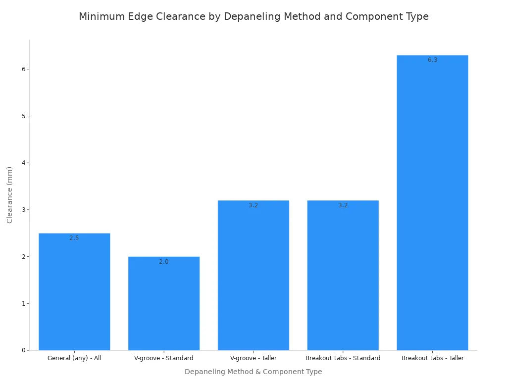
Putting parts too close to the edge of the board is one of the most common mistakes. When the factory cuts your board from the panel, the cutting process can break or chip parts near the edge. You need different spacing depending on the cutting method. V-groove scoring needs 0.075 inches for normal parts and 0.125 inches for taller parts. Breakout tabs need more space: 0.125 inches for normal parts and 0.250 inches for taller parts. A general rule of 0.100 inches works for any method.
Depaneling Method | Component Type | Clearance (inches) | Clearance (mm) |
|---|---|---|---|
General (any) | All | 0.100 | 2.5 |
V-groove | Standard | 0.075 | 2.0 |
V-groove | Taller | 0.125 | 3.2 |
Breakout tabs | Standard | 0.125 | 3.2 |
Breakout tabs | Taller | 0.250 | 6.3 |
Where you put connectors also matters for assembly. You want connectors easy to reach for testing and cable routing. Bad connector placement causes awkward cable bends or makes test probes hard to reach. Think about how someone will build and test your board before you lock in the positions.
Optimizing Placement for Signal Flow and Thermal Relief
Wrong part placement creates signal quality problems that are hard to find later. Putting high-speed parts far apart makes traces longer and hurts signal quality above 100 MHz. Group parts that work together. Keep decoupling capacitors within 5 mm of the power pin. If you ignore return path design when placing parts, you increase the current-loop area. This makes electromagnetic coupling and ground bounce worse.
Heat management also needs attention. Putting parts that make heat on the bottom layer stops natural airflow because warm air cannot rise. This trapped heat builds up and creates hot spots. Putting too many parts on the board makes the problem worse by packing heat sources in small areas.
To stop hot spots, spread heat-making parts evenly across the board. Packing parts too close together directly adds to heat buildup and shortens the board's life.
Put high-power parts near the board edges for better airflow. Keep heat-sensitive parts away from high-power devices. Use many thermal vias under high-power parts to move heat to other layers. Large copper areas spread heat evenly across the board. Bad via placement and routing under hot parts blocks this heat path, so plan your vias early. These heat management steps cost nothing during layout but save you from early board failures.
Ignoring Design for Manufacturability (DFM)
Design for manufacturability means you make the board so factories can build it without problems. Many designers skip this step. They focus on making the circuit work. They do not think about how the factory will build the board. This is one of the most costly pcb design pitfalls. You can avoid it by learning common violations and running proper checks.
Common DFM Violations That Halt Production
Factories reject boards for specific reasons. Know these violations before you send files.
DFM Violation Category | Specific Violation | Production Impact |
|---|---|---|
Insufficient Spacing | Trace-to-trace or pad clearances in dense areas | Shorts, etching defects, unreliable solder joints |
Insufficient Spacing | Component-to-annular-ring clearance | Assembly interference or solder reliability issues |
Insufficient Spacing | V-score to copper features | Board damage during depanelization |
Incorrect Hole Sizes | Inadequate spacing between holes | Drill damage or plating contamination |
Incorrect Hole Sizes | Insufficient annular ring (tight drill-to-pad tolerance) | Breakout or tangency |
Silkscreen Over Pads | Overlapping silkscreen with pads or copper features | Solder mask coverage issues, poor solderability |
Other violations also stop production. Floating copper pieces create shorts during assembly. Starved thermals cause incomplete connections. Missing clearance pads on pins connect all voltage planes together, creating shorts. Insufficient annular ring around a drilled hole can break the connection completely.
Over-specification causes delays. You specify trace widths beyond standard abilities. The factory sends engineering change requests. Complex stack-ups with blind vias freeze production if you have not checked availability. Incomplete fabrication docs cause 2-4 day delays. Missing or conflicting Gerber data makes the factory pause production. These are common pcb design mistakes you can prevent.
Running a Successful DFM Check
Run DFM checks throughout your pcb layout design. Start early. Check as you go.
First, submit your design files for review. Include the assembly doc, Bill-of-Materials, and Gerber files. The production team reviews your files. They inspect technical specs and manufacturing needs. They find potential issues early. They give a detailed report with helpful tips. The report covers areas to improve, design issues, and cost-saving ideas. You update your design based on these tips. Then manufacturing starts.
Ask yourself key questions during design. Can machines place your parts easily? Do you have enough clearance for soldering? Are you using factory-approved materials? Can test probes reach all test points?
Design for manufacturability is an ongoing process. Check each layer as you finish it. Run design rule checks after every major change. This prevents rework later.
Failing to account for manufacturing limits is a design for fabrication mistake that costs you time and money. A strict DFM checklist cuts rework rates a lot. One company dropped their rework rate from 10% to under 2% after using a proper checklist. They saved thousands and shortened their timeline by two weeks.
Design for manufacturability should guide every choice. From part placement to trace routing to stackup choices, think about how the factory will build your board. This mindset prevents pcb design pitfalls and ensures your first prototype works as expected.
Poor PCB Stackup Planning in Multi-Layer Boards
Your stackup defines how every layer of your board works together. Many designers treat it as an afterthought. They route traces first and think about layer arrangement later. This approach creates serious problems. Poor pcb stackup planning leads to signal integrity failures, manufacturing defects, and costly re-spins. You need to plan your layers before you place a single component.
The Risks of Poor PCB Stackup Planning
Signal integrity suffers when you ignore stackup planning. High-speed signals need a nearby ground plane for a clean return path. Without one, return currents travel longer routes. This increases loop inductance and causes voltage spikes or signal delays. Signal reflections occur when impedance mismatches appear along a trace. These reflections degrade signal quality and make your board unreliable.
Via stubs create another hidden problem. A via stub longer than 10 mils can introduce significant signal degradation. When a signal travels through a via, the unused portion acts like an antenna. It reflects energy and distorts the waveform. You must plan layer transitions carefully to minimize stub length.
Manufacturing problems also stem from poor stackup choices. Exceeding an aspect ratio of 10:1 for vias leads to unreliable boards. Press-fit connectors and high pin count BGAs fail when via aspect ratios exceed this limit. Warping or bowing occurs when you stack layers asymmetrically. Unbalanced copper distribution causes uneven expansion during lamination. Copper delamination happens when you bond incompatible materials without proper specifications.
Improper Stackup Planning Mistake | Manufacturing Problem Caused |
|---|---|
Designing before finalizing stackup | Impedance is wrong, via design is off, layer rework required |
Treating fabricator as an afterthought | Spec unavailable materials or exceed fab limits → delays and cost spikes |
Scattered/inconsistent documentation | Different files reference different stackups → re-spins and reliability failures |
A balanced (symmetric) stackup is significantly easier to predict during heat-intensive processes like lamination and solder reflow. In contrast, an asymmetric stackup is far more likely to encounter thermomechanical failures, specifically via barrel cracking and warpage, due to mismatches in the coefficient of thermal expansion (CTE) across the board layers.
Best Practices for Successful Multi-Layer PCB Design
You can avoid these pitfalls with a systematic approach to pcb stackup design. Start by defining your impedance requirements early. Controlled impedance traces need specific dielectric thickness and copper weight. You cannot guess these values after routing. You must calculate them before layout begins.
Maintain symmetry in your layer arrangement. A balanced stackup prevents mechanical stress during manufacturing. Place ground planes near high-speed signal layers. This provides a stable return path and reduces electromagnetic interference. Route high-speed signals first on layers adjacent to reference planes. Save lower-speed traces for other layers.
Use simulation tools to model signal behavior. These tools catch crosstalk and impedance mismatches before you send files to fabrication. Account for manufacturing tolerances in your calculations. Variations in material thickness or trace etching can affect impedance by up to 5-10%. Design with a buffer to absorb these variations.
Your pcb design multilayer strategy should include proper via planning. Keep via aspect ratios below 10:1. Place vias strategically to avoid signal delays and reflections. Poor via placement causes manufacturing challenges that you cannot fix with software.
Send your calculated stackup data to the fabrication house. Manufacturers need to verify their process can achieve your target impedance values. They use your dielectric thickness, copper weight, and trace width data to adjust their process parameters. If material thicknesses deviate from your design, they may change trace widths or recommend different dielectrics. This communication ensures your final board performs as intended.
Treat pcb stackup design as a continuous conversation with your fabricator. Share your layer ordering, material choices, and impedance targets early. Ask about their standard capabilities. This collaboration prevents delays and cost spikes. A well-planned multi-layer pcb design saves you time, money, and frustration. The best practices for successful multi-layer pcb design all point to one principle: plan your stackup before you route, not after.
Incorrect Decoupling Capacitor Placement
Decoupling capacitors act like small power backups. They give integrated circuits quick bursts of current. This keeps voltage steady and cuts down high-frequency noise. When you put them near power pins, you lower trace inductance. This keeps power flowing evenly and protects power integrity.
The Role of Capacitors in Power Integrity
Every time an IC switches states, it pulls a sudden burst of current. This happens in nanoseconds. Without a nearby capacitor, the voltage at the power pin drops. This drop can cause random microcontroller resets or unpredictable logic errors.
Bad placement causes more than just voltage drops. You might see ground bounce, where the ground reference shifts unpredictably. Signal problems show up as jitter, ringing, or crosstalk. Power traces act like antennas, sending out electromagnetic interference that fails EMC tests. These issues pile up fast in high-speed designs.
Putting capacitors too far from the IC adds parasitic inductance. A 2mm trace stub adds about 1 nH of inductance. This shifts the self-resonant frequency down, killing the high-frequency decoupling benefit. When you mix different capacitor values without care, you create anti-resonance spikes in the power distribution network impedance. These spikes boost noise instead of reducing it.
Placement and Routing Rules for Effective Decoupling
You need a clear plan for capacitor placement. Follow these rules to keep inductance low:
Use several capacitors in parallel. This gives lower effective series inductance than one capacitor.
Put capacitors closer to the IC for fast edge rates. This shortens the distance between capacitor and load.
Connect capacitors straight to power and ground planes via vias. Avoid long traces that add inductance.
Route back into interior layers instead of surface layers. This keeps loop inductance minimal.
A capacitor on the opposite side of a 1.6mm board adds 0.5–1.2 nH per via transition. Daisy-chaining power and ground vias multiplies total loop impedance. This weakens every capacitor in the chain.
For frequency coverage, use a mix of values. A 0.1μF capacitor alone leaves high-frequency noise unaddressed. Combine different values to cover multiple frequency ranges. This stops ground bounce and keeps power distribution issues away.
Ignoring power distribution during layout creates problems you cannot fix later. You must plan decoupling from the start. Measure your results after assembly. A well-decoupled board shows cleaner signals and lower noise. The effort pays off in reliable operation.
Inadequate Ground and Power Plane Design
Your ground and power planes are the base of your PCB's electrical performance. A bad ground plane design causes return current problems and raises electromagnetic interference. You need to know the risks and make solid planes from the beginning.
The Dangers of Split Planes and High Impedance Paths
Split planes break the return path for your signals. At high frequencies, current takes the path of least inductance under the signal trace. When you split the ground plane, that path is broken. The return current has to go around the gap. This makes the loop area and inductance bigger. The bigger loop works like an antenna, giving off noise.
Lee Ritchey says that cutting ground planes creates an EMI problem. A split plane makes digital return currents go around gaps, causing voltage drops on analog parts. The gap acts like a slot antenna. Signals that cross splits raise noise by 20 dB or more. High impedance return paths cause ground bounce and voltage drops that hurt signal integrity.
Impedance discontinuity is another big problem. Splits in the return path cause impedance that is not steady. When impedance changes, signals bounce back toward the source. These bounces cause ringing, overshoot, and undershoot. The result is unstable circuits and random failures. One four-layer ADC board with split grounds had 10 mV ripple until stitching vias fixed the return paths. Bad thermal management comes from poor plane design.
Designing Solid Planes for Low Noise and EMI
Build a solid, unbroken ground plane on a separate layer. This gives a low-impedance reference for all signals. A continuous ground plane holds in electromagnetic fields and lowers noise. At frequencies above 1 MHz, connecting ground at many points to a solid plane is the best strategy. A solid ground plane also helps with heat flow.
Place power and ground planes as close as you can, ideally less than 10 mils apart. This makes the capacitance between planes as high as possible for high-frequency decoupling. For every signal layer, put a reference plane next to it. This pair makes a controlled-impedance setup.
When signals change layers, put stitching vias near the signal via to connect the reference planes. Use grounded copper pours on outer layers with many stitching vias to the inside ground plane. A floating copper pour acts like an antenna and makes EMI worse.
Do not split ground planes. Use one single continuous reference plane. If you must split them, bridge the gaps with capacitors. These steps ensure electromagnetic compatibility. Good heat spread depends on solid planes. Designing with a continuous ground plane makes signal integrity better.
These six pcb design pitfalls all come from not enough planning at the start. Trace width errors, bad placement, DFM issues, weak stackups, poor decoupling, and broken planes happen because of rushed choices. You can avoid them with a step-by-step review before fabrication.
Prevention costs less than fixing later. A checklist catches common pcb design mistakes before they become re-spins. Avoid over-complex designs that strain factory limits. Keep your stackup balanced, planes solid, and capacitors close.
Adopt a structured design review process. Check each layer, run DFM reports, and test as you refine your layout. Master these basics, and your custom pcb projects will ship reliably on the first pass.
FAQ
What is the most common PCB design mistake?
Trace width errors cause the most failures. You must calculate current capacity using IPC-2221 before layout. Impedance-controlled traces need different calculations. Set up design rules in your CAD tool first to prevent overheating and signal issues.
How do I prevent a PCB re-spin?
Use a structured checklist before sending files. Check trace widths, component placement, DFM rules, and stackup symmetry. Run DFM checks throughout design. One company cut rework from 10% to 2% by using a proper checklist.
Why must decoupling capacitors sit close to IC pins?
IC switches pull current in nanoseconds. Without a nearby capacitor, voltage drops cause resets or logic errors. A 2mm trace stub adds 1 nH of inductance. Place capacitors within 5 mm of the power pin for clean power delivery.
What happens if I split the ground plane?
Split planes break return current paths. At high frequencies, current takes the path of least inductance under the signal trace. Gaps create larger loop areas that radiate noise. Use one continuous ground plane instead.
See Also
Preventing Typical SMT Assembly Flaws in Circuit Boards
Enhancing PCBA Durability for Sustained Operation Through Key Measures
Steering Clear of Frequent Errors During BGA Assembly Processes
Critical SMT Assembly Concerns for VIPPO-Equipped PCB Boards
Accelerating Project Efficiency via Rapid PCB Assembly Prototypes
