EMI/EMC Considerations in PCBA Design
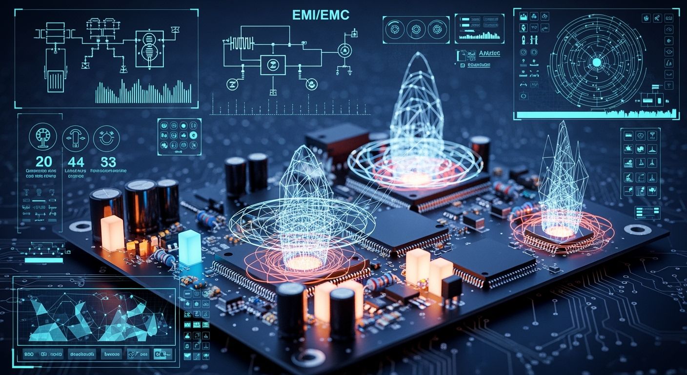
When designing a PCBA, it's crucial to consider EMI/EMC considerations. Ignoring these factors can lead to significant issues. Some companies have faced product recalls or hefty fines due to neglecting EMI/EMC considerations. They might even be prohibited from selling in regions such as the EU or US, which can harm their reputation and result in financial losses. Proper EMI/EMC considerations ensure compliance with regulations and maintain product reliability. They also prevent costly problems. By making informed design choices, you can reduce risks and enhance the safety and quality of electronics.
Key Takeaways
Learn about EMI and EMC so your device works well. EMI and EMC help stop problems with interference. Think about EMI and EMC when you design to avoid recalls and fines. Use smart PCB layout and grounding to lower EMI and make your device more reliable. Keep noisy circuits away from sensitive circuits to stop interference. Begin EMC checks early to save time and money.
EMI/EMC Considerations in PCBA
EMI and EMC Definitions
It is important to know about emi/emc when you work with a pcb. EMI means electromagnetic interference. This happens when signals mess up how your circuit works. EMC stands for electromagnetic compatibility. This means your device can work well without causing or getting too much interference. When you design a pcb, you need to make sure your product follows both emi and emc rules. This helps your device stay safe and work the right way.
Impact on Reliability and Compliance
If you do not think about emi/emc, your pcb can have lots of problems. EMI can make devices stop working or act weird. In important areas like medical devices or airplanes, even small emi problems can cause big trouble. The table below shows how emi can hurt reliability over time:
Critical Factors | Description |
|---|---|
Latent Defects | Problems can show up weeks or months later if not found early. |
Thermal Fatigue | Bad solder joints get weaker when temperatures change. |
Electromagnetic Interference (EMI) | Bad solder joints can cause emi, which is very bad for satellites. |
Inspection Tools | 3D SPI works best; 2D visual checks do not work as well. |
You also need to care about following the rules. Many products fail checks because of simple mistakes. These mistakes are:
Cables that are too long
Wrong ways to use shielding
Not doing pre-compliance testing
If you skip emi/emc steps, your product might not pass emc rules. This can stop you from selling your product in many places. You could also have to recall your product or pay fines. If you pay attention to emi/emc, your product will work better and pass emc checks.
EMI Sources in PCBAs
Internal Circuitry and Switching
It is important to know how your pcb makes emi. The circuit inside can create emissions when signals switch fast. These signals make noise and send out emissions. Metal parts can act like antennas. They send out electromagnetic interference and make more noise. If signal return paths are bad, signals stretch across the board. This makes more noise and emissions. When traces are close, crosstalk happens. One circuit can mess up another. You will see interference and noise in your pcb. Both high-frequency and low-frequency signals can cause trouble. Fast switching in digital circuits makes radiated emissions. Analog circuits can also make noise if not designed well.
Tip: Keep traces short and apart. This helps lower crosstalk and noise.
Here is a simple list of common emi sources inside a pcb:
Antennas: Metal parts act as antennas and increase emi.
Return Paths: Bad signal return paths make noise and emissions.
Crosstalk: Close traces cause circuits to interfere.
Environmental Interference
Your pcb also gets emi from outside sources. Electromagnetic waves from radio transmitters can mess up your circuit. Industrial machines send out emissions. These emissions cause noise and interference in your pcb. Thunderstorms and high-voltage lines add more noise. Radar systems, wireless devices, and radio transmitters all make electromagnetic interference. You need to protect your pcb from these outside factors. If you do not, your circuit will have noise and emissions.
Note: Keep your pcb away from strong radio transmitters and big machines. This helps reduce interference.
You can see how outside interference affects your pcb in this table:
Source | Effect on PCB |
|---|---|
Radio transmitters | Mess up circuit, make noise |
Industrial equipment | Make more radiated emissions |
Thunderstorms | Add noise and interference |
High-voltage lines | Cause unwanted emissions |
EMI/EMC Design Strategies
If you want your pcb to pass emc tests, you need to use smart design strategies. These strategies help control emi and lower noise. They also help you follow emc rules. You will see your pcb work better and have fewer problems. Using the right layout, grounding, partitioning, and shielding makes a big difference.
PCB Layout and Grounding
Good pcb design starts with smart layout and grounding. Always use a solid ground plane. This ground plane gives return currents a clear path. It keeps impedance low and stops emi from spreading. If you skip the ground plane, you might see voltage drops and noise. This can cause data errors and make your pcb fail in high-speed jobs.
Here are some easy pcb design tips for layout and grounding:
Put a ground plane under signal layers. This keeps return paths short.
Place the ground plane close to the signal layer. This lowers emi by making the return path shorter.
Use star grounding in mixed-signal designs. Connect all ground points to one spot. This keeps noise away from sensitive circuits.
Add lots of vias for ground connections. This is important for high-frequency chips. It lowers inductance and helps control emi.
Keep power and ground planes apart. This makes a low-inductance path for decoupling and keeps power steady.
Do not use right-angle bends in traces. Keep traces short and straight to lower emi.
Group similar functions together. Put decoupling capacitors close to chips to block noise.
Tip: A solid ground plane helps keep signals clean and stable. This is very important for emc.
Component Placement and Shielding
Where you put parts on the pcb matters for emi and emc. Follow emc rules for placing and grouping parts. Start by putting connectors on the edge of the board. Place esd and circuit protection parts near these connectors. Next, add main chips like microcontrollers. Put decoupling capacitors close to them. Mount passive parts, like resistors, after that. Make sure similar parts face the same way. This makes routing easier and helps with assembly.
Follow these steps for better pcb design:
Put connectors and protection parts at the edge.
Add main chips, then decoupling capacitors.
Mount passive parts.
Line up similar parts for easy routing.
Leave space between parts to avoid redesigns.
Think about partitioning too. Use circuit partitioning to keep digital, analog, and power sections apart. This stops noise from jumping between blocks. Partitioning keeps noisy circuits away from sensitive ones. Good partitioning keeps signals strong and emi low.
Shielding is another important part of pcb design. You can use metal covers, guard traces, or shielded cables to block emi. Shielding works in three ways:
Mechanism | Description |
|---|---|
Reflection | Bounces emi away, but gaps in the shield can let noise through. |
Absorption | Uses materials like steel or ferrite to soak up emi and turn it into heat. |
Multiple Reflections | Scatters emi inside the shield, making it weaker before it can escape. |
Note: Shielding works best when you use good grounding and partitioning.
Filtering and Isolation
Filtering and isolation are strong tools in pcb design for emi and emc. You can use emi filters to block unwanted noise on power and signal lines. The most common filter is the low-pass filter. It lets low-frequency signals pass but blocks high-frequency emi. You can use resistors, ferrite beads, or special emi filters for this job. Ferrite beads block high-frequency noise but let dc signals through. Common-mode chokes are also useful. They stop noise on both wires of a pair but let the real signal pass.
Picking the right emi filter is important. You can choose active or passive filters, panel mount filters, or suppression filters. Match the filter to the type of noise you want to block. For example, use a differential mode filter for noise between two lines. Use a common mode filter for noise on both lines.
Isolation is just as important as filtering. Keep digital, analog, and power circuits apart. This is called circuit partitioning. When you separate noisy circuits from sensitive ones, you stop noise from spreading. Use clear boundaries between blocks. This keeps signals clean and emc strong.
Remember: Good filtering and isolation make your pcb design much stronger against emi.
By using these pcb design strategies—solid ground planes, smart grounding, careful partitioning, shielding, and strong filtering—you can control emi and follow emc rules. These steps help your pcb pass emc tests and work well in real life.
Design for EMC Compliance
Pre-Compliance Simulation
You can use pre-compliance simulation tools to help with emc compliance. These tools let you find emi problems before making your pcb. Simulation shows how your design will do in emissions and immunity tests. You can fix problems early by changing layout, shielding, or where you put parts.
Many engineers use special software to check emc compliance. Here is a table with some popular tools and what they do:
Tool Name | Application |
|---|---|
Ansys SIwave | Finds and fixes emi, checks signal integrity and PDN noise. |
Cadence Sigrity | Looks at fast traces and predicts emi. |
Ansys EMC Plus | Tests for emc and helps with certification for different standards. |
Ansys EMC Plus lets you test your pcb for rules like CISPR and MIL-STD. You can try different designs and make your pcb better for emc compliance. Simulation tools help you check emissions and immunity before building your board.
You should look at important things during pre-compliance simulation. The table below shows what to test:
Test Type | Description |
|---|---|
Emissions Testing | Checks how much electromagnetic emissions come from your device. |
Immunity Testing | Checks how your device handles outside electromagnetic interference. |
Radiated Testing | Measures emissions sent out as electromagnetic waves. |
Conducted Testing | Measures emissions that go through cables and connectors. |
If you use simulation early, you can save money and time. You can work with emc experts to make smart changes. Early testing helps you pass emc tests the first time.
Tip: Start simulation when you plan your system. This helps you find emi and emc problems before they cost a lot.
EMC Testing Methods
After simulation, you need to test your pcb for emc. Testing checks if your design meets emc rules. There are different ways to test emissions and immunity.
Here are the most common emc testing methods used today:
Radiated Emissions Testing checks electromagnetic waves from your pcb. You compare results to rules like CISPR 32.
Conducted Emissions Testing checks noise on power lines. You use rules like CISPR 11.
Radiated Immunity Testing puts your pcb near electromagnetic fields. You see if your device keeps working.
Conducted Immunity Testing checks how your pcb handles noise on power and signal lines.
ESD Testing simulates static discharge to see if your pcb is strong.
You also need to test for other emi types. Here is a list of extra emc testing methods:
Electrostatic Discharge (ESD) simulates static from people or devices.
Electrical Fast Transient (EFT) simulates quick bursts from switching.
Surge Immunity copies surges from lightning or power grid problems.
Radiated/Conducted RF Immunity tests how your pcb handles strong RF fields.
You should do pre-compliance testing before the final emc tests. Early testing helps you find and fix emi problems. If you wait too long, you might fail tests and delay your product. You can use shielding and change your pcb layout to stop emi problems.
Note: Think about emc compliance from the start. This helps you pass tests and avoid doing your design over.
EMC Standards Overview
You must follow emc rules from around the world when you design your pcb. These rules set limits for emissions and immunity. If you meet these rules, you can sell your product in many places.
Here is a table with main emc rules for consumer and industrial pcbas:
Governing Body | Standard | Description |
|---|---|---|
FCC | 15 | Broadcast receivers |
EN | 55013 | Household appliances/tools |
CISPR | 13 | Fluorescent lights/luminaires |
FCC | 18 | Industrial, scientific, and medical equipment |
EN | 55022 | Information technology equipment |
EN | 61000-6-3,4 | Generic emissions standards |
You need to know which rule fits your product. For consumer products, radiated emissions are usually the hardest. Industrial equipment needs to focus on conducted emissions and cable immunity. Cars must meet all emc rules because they need to be very reliable.
Rules like CISPR 22 and FCC Part 15 set emissions limits. There are seven CISPR and EN rules that match FCC Part 15. Each rule has its own emissions needs. You should start thinking about emc at the system planning stage. Picking the right parts early helps you meet emc rules.
Tip: Always check the newest emc rules for your product. This helps you avoid fines and product recalls.
If you follow emc rules and use simulation and testing, you can make a pcb that passes emc. You will have fewer emi problems and your product will work well.
Practical Tips and Pitfalls
Actionable Design Tips
You can make your pcb better against noise by using some easy steps. First, keep noisy circuits away from sensitive ones. Put switching regulators, clocks, and RF circuits far from analog circuits and sensors. This stops noise from spreading to other parts. Use metal shields for parts like oscillators and RF modules. Connect these shields to the ground plane for best results. Put guard rings around sensitive traces. Use ground fills on the outside layers to block extra noise.
Pick laminates that have a steady dielectric constant. This helps keep impedance steady and lowers noise. Use thin dielectrics between power and ground layers. This makes more capacitance and cuts down on emissions. For fast circuits, use low-loss materials to stop signal loss and radiation.
Check your design early in the process. Use pre-compliance tests with near-field probes to find noisy spots. Lab tests will show if your pcb meets emc rules. Review your design early to catch emc problems before they get big. Looking at schematics and layouts early saves time and money.
Tip: Keep digital and analog circuits apart. Always check your design for emc problems from the start.
Common Mistakes to Avoid
Many engineers make the same mistakes with emc in pcb projects. Here are some common errors and how to avoid them:
Not planning the return path. If you break the return path, your pcb can act like an antenna and make more noise.
Forgetting about ground quality. Broken grounds cause bad references and more noise.
Messy power networks. Bad decoupling causes voltage ripple and more emissions.
Bad high-speed routing. Sharp corners and long stubs turn traces into antennas.
Waiting too long to add shields or filters. Fixing emi after layout is hard and does not work well.
Remember: Fix emc and noise problems early in your design. This helps you avoid expensive changes and keeps your circuit working well.
You can get strong emc performance by making smart design choices. Start thinking about compliance early in your project. Good emc design helps you avoid big mistakes. It keeps your products working well. If you manage emc early, you get many benefits for a long time:
You can get your product to market faster.
You use your engineering resources better.
You improve cost and performance without rushing emc fixes.
You lower your risk of problems.
Bad emc design can cause expensive redesigns and product recalls. It can hurt your reputation. Stay proactive and keep learning about new emc standards. This protects your products and your business.
FAQ
What is the main cause of EMI in PCBAs?
You often see EMI from fast switching signals, long traces, or poor grounding. High-speed digital circuits and power converters create most EMI problems. Careful layout and good grounding help reduce these issues.
How can you quickly check for EMI problems?
You can use a handheld near-field probe to scan your board. This tool helps you find noisy spots before full EMC testing. Early checks save time and money.
Do you always need shielding for good EMC?
No, you do not always need shielding. Good layout, grounding, and filtering often control EMI. Use shielding when you have strong noise sources or sensitive circuits.
Which EMC standard should you follow?
You should check the product type and where you plan to sell it. For example, FCC Part 15 covers most consumer electronics in the US. EN 55032 applies in Europe.
See Also
Understanding PCBA Processing Needs for Medical Devices
Defining PCBA: Its Meaning in the Electronics Field
Essential Strategies to Enhance PCBA Reliability Over Time
