How PCB Trace Width Impacts Current Capacity and Safety

You need to know how pcb trace width changes current and safety. If you pick a trace that is too thin, it can get too hot and break. Wider traces let heat spread out, so more current can move safely. Thicker traces lower resistance and stop too much heat. Longer traces can make resistance go up, so heat can build up. You should always think about the air temperature, because it affects how much heat your pcb can take.
Key Takeaways
Wider PCB traces let more current move safely. This helps stop overheating and damage. - Always pick a trace width that fits your design’s current needs. This keeps your PCB safe and reliable. - Use IPC-2152 standards and online calculators to find the right trace width for your PCB. - Think about copper thickness. Thicker traces carry more current with less resistance and heat. - Keep enough space between traces. This stops short circuits and overheating when using high current.
PCB Trace Width Basics
What Is PCB Trace Width?
You can think of pcb trace width as the size of the copper path that carries electricity on your pcb. This path acts like a tiny wire printed on the board. The width of the trace decides how much current can safely flow through it. If you make the trace too narrow, it will have more resistance. This resistance causes the trace to heat up when current passes through. Too much heat can damage the trace or even burn it off the board.
PCB traces do not act like perfect wires. They have some resistance, which limits how much current they can handle.
Every trace has a maximum current it can carry before it fails. The width of the trace is a key factor in this limit.
If you push too much current through a narrow trace, it can overheat, burn, or peel away from the pcb.
You should always choose a trace width that matches your current needs. This helps keep your pcb safe and reliable.
Measuring Trace Width in Mil and mm
You measure trace width using units like mils and millimeters (mm). One mil equals one-thousandth of an inch. Millimeters are part of the metric system. Many designers use mils for small traces because they give you more precise control. For example, a trace might be 10 mils wide, which is 0.254 mm.
The IPC-2221 standard gives a way to estimate how much current a trace can carry based on its cross-sectional area in square mils. However, IPC-2152 is a newer standard. It uses more modern testing and lets you use slightly smaller trace widths for the same current. This means you can design more compact pcbs without losing safety.
Tip: Always check which unit your pcb design software uses. Mixing up mils and millimeters can lead to mistakes in your layout.
Trace Width and Maximum Current Capacity
Relationship Between Trace Width and Current Capacity
It is important to know how trace width changes current capacity. Wider traces can carry more current because they have a bigger area. This bigger area lets electricity move with less resistance. When you make the trace wider, resistance goes down and heat spreads out better. This helps your pcb handle more current without getting too hot.
Here is a simple table that shows how different things affect maximum current:
Factor | Description |
|---|---|
Trace Width | Wider traces can carry more current without overheating, reducing resistance and heat generation. |
Copper Thickness | Increasing the cross-sectional area lowers resistance, enhancing current-carrying strength. |
Temperature Rise Limit (∆t) | A smaller allowable temperature rise needs wider traces to limit heating, affecting capacity. |
You can also look at how math shows the link between trace width and current:
The link between pcb trace width and maximum current can be shown as:
$I = \frac{A \times J}{1000}$
where:
$I$ is the current in Amperes (A)
$A$ is the cross-sectional area of the trace in square millimeters (mm²)
$J$ is the current density in Amperes per square millimeter (A/mm²)
For example, if you want to carry 10 A with a copper thickness of 2 oz (70 μm) and a current density of 4 A/mm², you need a cross-sectional area of 2.5 mm². This means your trace width should be about 35.7 mm.
You should always pick a trace width that matches the current you need. This helps stop problems and keeps your pcb safe.
Heat Generation and Overheating Risks
Trace width and current are important for safety. If you use a narrow trace for high current, resistance goes up. This makes the trace get hot. Too much heat can hurt your pcb or make the trace peel off.
Wider traces let more current flow and lower the chance of overheating.
If the trace is too narrow, resistance and heat go up, which can hurt the pcb.
Doing the right math for trace width keeps the temperature safe. This is very important for your pcb to last a long time.
You must always check trace width and current to stop overheating. If you do not, your pcb might break when used.
Minimum Trace Width Standards
You need to follow minimum trace width rules from pcb makers. These rules help you pick the right trace width for your current. The IPC-2221 standard gives steps for finding the minimum trace width using current, copper thickness, and temperature rise. It uses real data and math to make sure your traces can handle the most current without getting too hot.
Here is a table showing example minimum trace widths for 20A:
Standard | Description | Example Trace Width for 20A (1 oz copper, 10°C rise) | Example Trace Width for 20A (2 oz copper, 10°C rise) |
|---|---|---|---|
IPC-2221 | Provides guidelines for calculating trace widths based on current, copper thickness, and temperature rise. | 5.2 mm (205 mils) | 2.6 mm (102 mils) |
IPC-2152 | Offers more detailed data for trace width calculations. | N/A | N/A |
You should always use current tables and standards like IPC-2221 or IPC-2152. These help you pick the right trace width and area for your design. If you use traces that are too small, you risk overheating and problems in the field.
Tip: Always check the minimum trace width your pcb maker needs. This makes sure your design is safe and helps you avoid mistakes.
PCB Trace Thickness and Copper Weight
How Trace Thickness Affects Current Capacity
You need to understand how pcb trace thickness changes the way your board handles current. The thickness of copper traces comes from the copper weight used during manufacturing. Thicker traces have a larger cross-sectional area. This means less resistance and less heat when current flows. You get better reliability in all types of applications because thicker traces help keep your board cool and safe.
When you increase pcb trace thickness, you allow more current to move through the trace without overheating. For example, if you double the copper thickness, you can almost double the current capacity for the same temperature rise. This is important for power electronics, automotive, and industrial applications. You can use formulas to find the cross-sectional area and see how much current your trace can handle. Always remember, thicker copper means your pcb can work better in demanding applications.
Standard Copper Weights and Their Impact
Manufacturers measure copper weight in ounces per square foot. Each copper weight matches a certain thickness. Here is a table that shows common values:
Copper Weight | Thickness (approx.) |
|---|---|
0.5 oz | 17 µm (0.7 mil) |
1 oz | 35 µm (1.4 mil) |
2 oz | 70 µm (2.8 mil) |
3 oz | 105 µm (4.2 mil) |
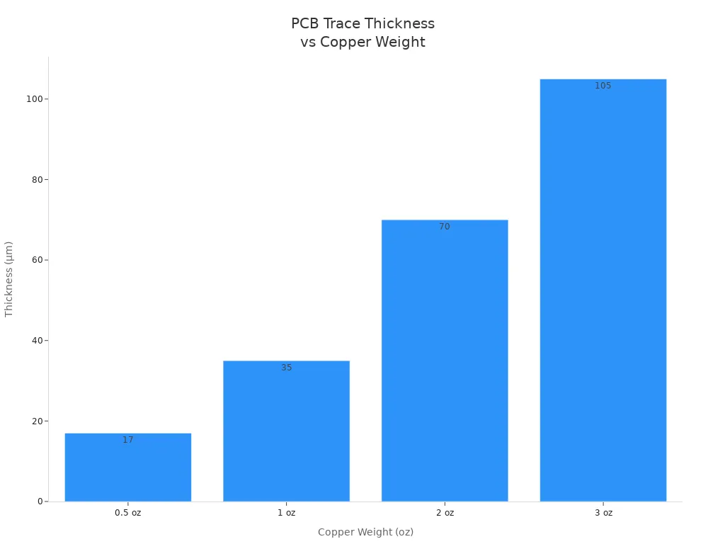
You will see 1 oz and 2 oz copper used in most pcb designs. Heavy copper pcb design uses 3 oz or more for high-power applications. When you use a higher copper weight, you get thicker traces. This reduces resistance, lowers voltage drop, and spreads heat better. You can carry more current with the same trace width. For example, a 1 mm wide trace with 2 oz copper can carry about 4.2 A with a 10°C rise, while the same trace with 1 oz copper handles only 2–2.5 A.
You should always match the copper layer thickness to your application. If your design needs to handle high current, choose a heavier copper weight. This will help your pcb last longer and work safely in all applications.
Trace Width Selection Guidelines
Using IPC-2152 and Current Tables
You can use IPC-2152 and current tables to help pick the right trace width for your pcb. IPC-2152 gives rules for how much current a trace can carry. It looks at things like copper weight, where the trace is, and how cool the board stays. It also checks other things that can change how much current the trace can handle. Here is a table that shows what you should think about:
Factor | Description |
|---|---|
Copper Weight | Thickness of the copper used in the PCB traces. |
Trace Location | Whether the trace is on an external or internal layer of the PCB. |
Cooling Environment | The external cooling conditions, such as air or vacuum. |
Thermal Conductivity | How well the PCB material conducts heat. |
Correction Factors | Adjustments for special situations like extra cooling or planes. |
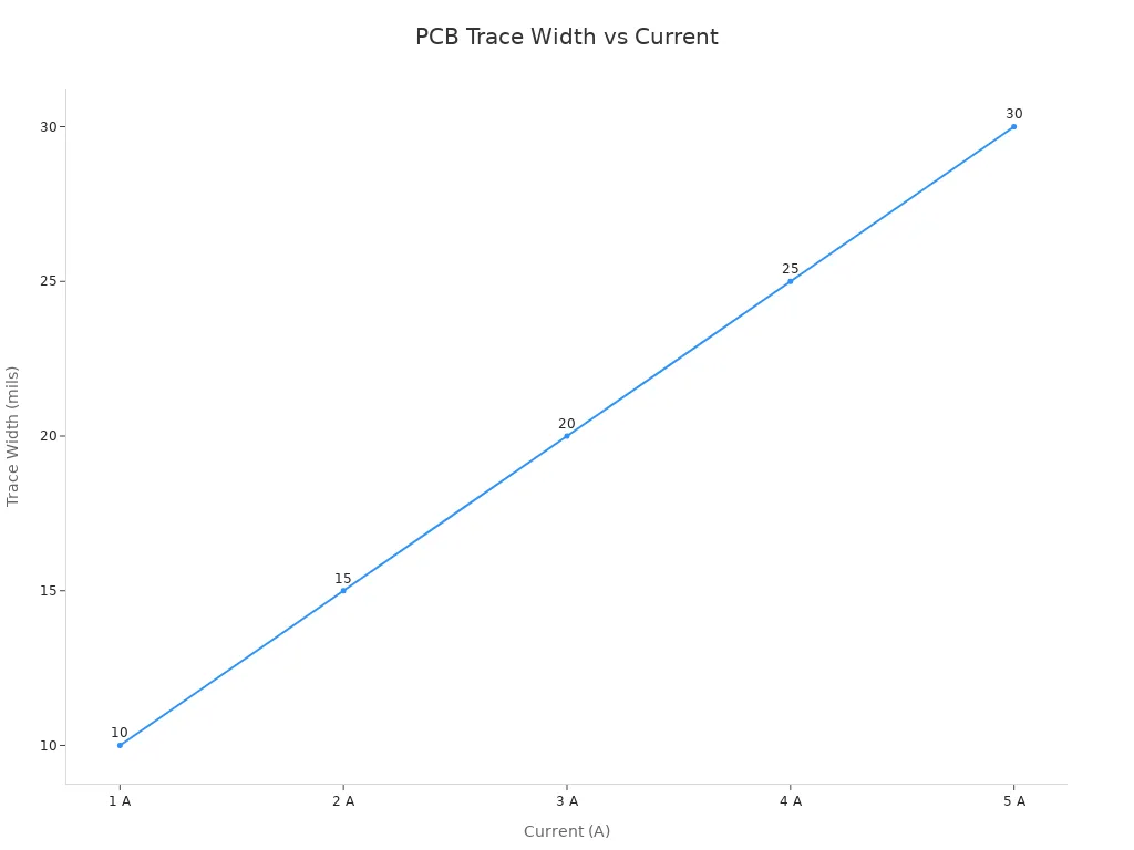
You can also use current tables to match your design needs. For example, if you want the trace to get only 10°C hotter, you can use this table:
Current (A) | Recommended Trace Width (mils) for 10°C Rise |
|---|---|
1 | 10 |
2 | 15 |
3 | 20 |
4 | 25 |
5 | 30 |
Calculation Methods for Trace Width
You can use pcb trace current math to find the best trace width. Many engineers use online calculators for trace width. These tools help you not make mistakes and save time. Doing the math by hand can work, but it takes longer and you might mess up. Here is a quick chart to compare:
Method | Accuracy | Time Efficiency | Error Prone |
|---|---|---|---|
Manual Calculation | Can be accurate | Time-consuming | Prone to error |
Online Calculators | Streamlined | Efficient | Less prone to error |
When you do the math, remember to check copper thickness, current, and how hot the trace gets. For example, a trace that carries 5A with 2 oz copper and a 15°C rise needs to be at least 55.3 mils wide. Always check the voltage drop and make sure it is less than 5% of your supply voltage.
Practical Tips for High-Current Designs
You should follow these steps for high power designs and high-power uses:
Find out the most current your trace will carry.
Pick the right copper weight for your pcb.
Set a safe temperature rise.
Use wider traces for power and ground paths.
Put thermal vias near hot spots.
Do not use sharp corners or skinny parts.
Use more than one via for high-current paths.
Tip: Test your board with real loads. Measure voltage drop and look for hot spots with a thermal camera.
If you do these steps, your pcb will meet your needs and stay safe.
Safety Best Practices
Preventing Overheating and Failures
You can keep your circuit from getting too hot by doing a few things. Wider traces make resistance lower and help heat spread out. Thermal vias near hot spots move heat away from the circuit. Using heavier copper layers helps your circuit carry more current and stay cooler. If you use more layers, you can share the heat and keep the circuit from overheating. You also need to think about the environment. High temperatures make resistance go up and can cause signals to get weaker. Humidity can make paths between traces and cause short circuits. You can use special coatings to protect your circuit from water.
Note: Picking the right trace width stops overheating and keeps your circuit safe. Wider traces let more current flow and lower the risk of problems from narrow traces.
Here is a table with best ways to stop overheating:
Best Practice | Description |
|---|---|
Utilize Multiple Layers | Spread high-current traces across layers to share heat better. |
Mitigate Temperature Rise | Use wider traces or thicker copper to lower resistance and heat. |
Consider Environmental Factors | Think about air temperature to stop too much heat. |
Incorporate Thermal Management | Use thermal vias and heatsinks to move extra heat away from important parts. |
Trace Spacing for High Current
You need to leave enough space between traces in your circuit. Good spacing stops sparks and short circuits. Clearance is the smallest air gap between conductors. For circuits over 50V, clearance starts at 1mm and gets bigger as voltage goes up. Creepage is the path along the pcb surface. Humidity and dirt can change creepage. Power circuits need 8–15 mil spacing for safety and to help heat move away. If you do not follow spacing rules, you can get sparks, shorts, crosstalk, and too much heat.
Aspect | Description |
|---|---|
Clearance | Smallest air gap between conductors; starts at 1mm for over 50V and gets bigger with more voltage. |
Creepage | Path along the pcb surface; humidity, dirt, and board material can change it. |
Power circuits spacing | Traces with lots of current need 8–15 mil spacing for safety, heat, and isolation. |
Consequences of inadequate spacing | Not enough space can cause sparks, shorts, crosstalk, and too much heat, which hurts performance. |
Ensuring Long-Term Reliability
You can make your circuit last longer by picking the right trace width for real use. Use thermal simulation tools to find hot spots and change trace width if needed. Add more vias to give current more paths to flow. Through-hole vias make a strong path for high-current traces. You should design cases with vents or fans to help air move. Materials that move heat well help your circuit last longer. Special coatings keep water away from traces and make your circuit more reliable. If you learn about signal integrity, power integrity, and thermal management, you can build circuits that work in tough places.
Tip: Heat and humidity can make electronic parts fail. You need to design your circuit to handle these things for the most current and long life.
You need to pick the right PCB trace width and thickness. This keeps your circuit safe and working well. Wider traces and thicker copper let more current flow without getting too hot. Using IPC rules and math helps stop your board from failing.
Always check trace width, copper thickness, and how hot it gets.
Use IPC-2152 to help you decide.
Leave extra space and keep power traces away from sensitive signals.
Put your current needs in a calculator.
Choose the right copper thickness.
Set a safe temperature rise.
Change trace width for space and safety.
Tip: Wider traces near power parts handle sudden spikes better and make your board last longer.
FAQ
What happens if you use a trace that is too narrow?
You risk overheating and damaging your board. Narrow traces cannot carry enough current safely. You may see burnt traces or failed connections in your printed circuit board assembly.
How do you choose the right trace width for circuit design?
You start by checking the maximum current your trace will carry. Use IPC-2152 tables or online calculators. Always match the trace width to your circuit design needs.
Does copper thickness affect current capacity?
Yes. Thicker copper lets more current flow with less resistance. You can use heavier copper for high-power traces. This helps your board stay cool and reliable.
Why is trace spacing important for high-current paths?
Trace spacing prevents short circuits and overheating. You need enough space between traces to keep your board safe. High-current paths require wider spacing to handle heat and avoid electrical problems.
Can you use online tools to calculate trace width?
You can use online calculators to find the best trace width. These tools help you avoid mistakes and save time. Always check your results with industry standards.
Tip: Always test your board under real conditions to make sure your traces stay safe.
See Also
Designing PCB Boards for Efficient SMT Manufacturing Processes
Essential Guidelines for Safe HDI PCB Assembly Practices
Fundamental Criteria for PCB Boards in SMT Production