ATM Machine PCBA Manufacturing Process
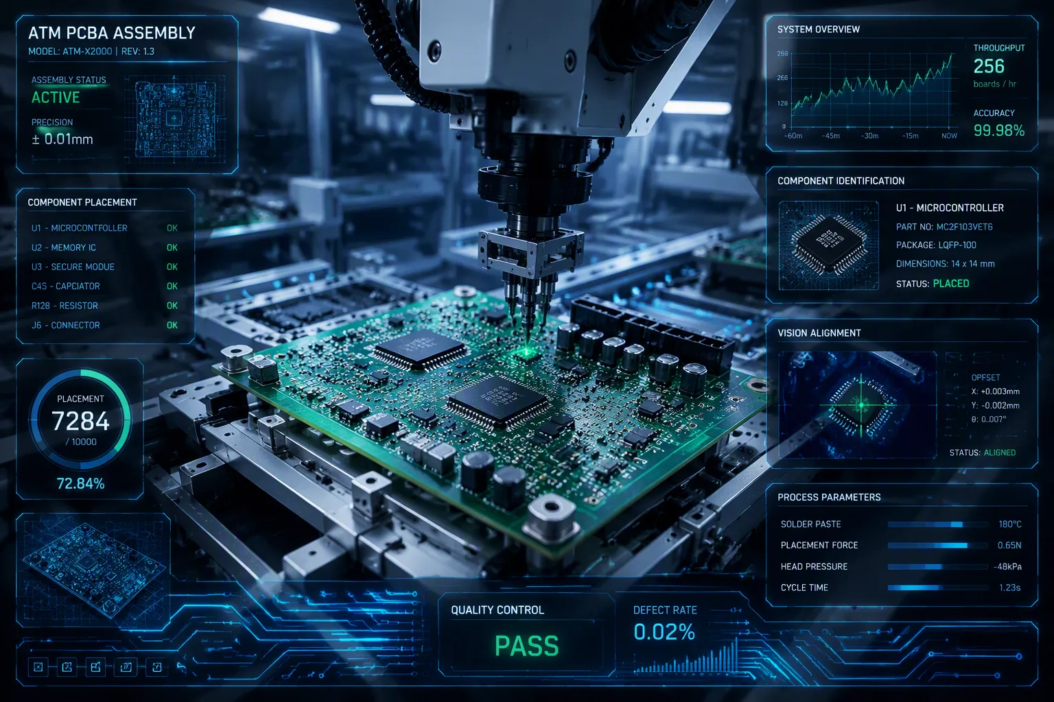
You see ATMs as silent guardians of your money. Behind the screen, a complex electromechanical system works. At its heart lies the pcba. This part needs exceptional precision and security. The PCBA Manufacturing process is a multi-stage journey from design to testing. The process starts with a pcb. Each stage requires careful planning and execution. The pcb layout must account for outdoor conditions. The materials must handle temperature changes and physical stress. Security features are built directly into the pcba. The result is a board that protects financial data for years. This journey ensures the reliability you trust. Let's explore the critical steps of manufacturing.
Key Takeaways
Use high-Tg laminates and thick copper to handle outdoor temperature changes and moisture.
Place DC-DC converters near loads and use decoupling capacitors for steady, quiet power.
Use SMT machines with ±25 μm accuracy and controlled reflow profiles to make sure the solder joints are reliable.
Run HALT, thermal shock, humidity, and vibration tests to find failures before sending the product out into the field.
Add tamper-proof coatings and encryption chips to meet PCI-DSS rules and keep financial data safe.
The Foundation of PCBA Manufacturing
Design and Material Selection
The pcba manufacturing process starts long before assembly lines run. First, you turn design files into a real board. This step is very important in the whole pcba making workflow. The design must plan for every part's location, trace width, and layer stack-up. Engineers use special software to test heat and electricity behavior before making the board.
Material choice needs careful thought. ATMs often sit outside, so they face temperature changes and physical stress. Normal boards fail in these conditions. You need circuit boards made from materials that can handle very hot, cold, and wet weather. High-Tg (glass transition temperature) laminates stop warping when it gets hot. Thicker copper layers carry more current without overheating. The circuit board material must also resist water absorption, so it does not split apart after years of use. Each material choice affects how long the board lasts and how reliable it is.
Power Management and Layout
Power management shapes the whole board layout plan. An ATM has many parts that need different voltage levels, such as for the main processor, sensors, and motors. You cannot send raw power straight to these parts. High-efficiency DC-DC converters, working above 90% efficiency, cut down power loss and heat. This efficiency keeps stable voltage all over the board.
Where you place parts matters just as much as picking them. You put the converter close to the load to lower trace resistance and inductance. This closeness stops voltage drops when loads change. Filtering capacitors, from 10 μF to 100 μF, smooth output ripple to below 50 mV. Sensitive parts need this clean power. The board layout also uses decoupling capacitors—0.1 μF near each IC and 10-47 μF bulk capacitors—to keep noise below 1% of the supply voltage. Low quiescent current, below 100 μA, cuts standby power use. This design keeps steady performance even when idle. The whole manufacturing process depends on these basic choices, so the final board works perfectly for years.
The PCB Manufacturing and Assembly Process
You now move from design to the physical build. The pcb manufacturing process begins by turning your board into a working pcba. The pcb assembly process needs accuracy at every step. You apply solder paste, put parts in place, and solder them. Each step builds on the last to make a reliable pcb.
Solder Paste and Component Placement
The first step in the pcb assembly process is solder paste screening. You put solder paste on the bare pcb through a stencil. The stencil has holes that match the pad locations. This method puts paste only where you need it. The pcb gets paste exactly where required. The paste has tiny solder balls mixed with flux. The flux helps clean metal surfaces and helps bonding. Your pcb now has paste ready for parts.
You choose parts before placement. You pick standard parts like SOIC, QFP, or BGA packages. These parts have matching footprints and cut down lead times. You think about thermal resistance and derating rules. This stops overstress during use. Keep good spacing between parts. This spacing stops soldering defects and allows fixes later. You also follow electrical clearance and creepage distance rules. This stops arcing between conductors.
The placement stage uses surface-mount technology (SMT) machines. These machines pick parts from reels or trays. They put each part with high accuracy on the paste. The SMT placement machines have a placement accuracy of ±25 micrometers. They handle parts as small as the 01005 package size. This accuracy works at high speeds. The machines place tens of thousands of parts per hour. Speed and accuracy make your pcb assembly process run well. The pcb manufacturing line depends on this ability. Each pcb moves through the line with care.
You also think about trace routing during this phase. Use wide, well-spaced traces for good current flow. Controlled impedance routing helps fast signals. This cuts down reflections and crosstalk. Material selection matters too. Choose laminates with the right glass transition temperature (Tg) and coefficient of thermal expansion (CTE). Use conformal coatings for harsh conditions. Thermal management uses thermal vias, heat sinks, and copper pour areas. These parts move heat away from important components. Include test points and boundary scan (JTAG) for testing. This helps with final inspection later.
Reflow Soldering and Inspection
After placement, the board moves to reflow soldering. The pcb assembly process now uses a reflow oven. The oven heats the pcb in a controlled temperature profile. The solder paste melts and makes permanent connections. The temperature profile has several zones. The preheat zone slowly raises the pcb temperature. The soak zone turns on the flux. The reflow zone melts the solder. The cooling zone hardens the joints. This whole assembly step needs careful tuning. Wrong temperatures can cause defects.
After reflow, you check the pcb. Automated optical inspection is the first check. AOI uses cameras to scan the whole pcba. The system compares each pcb to a golden reference. It finds many types of defects. Common defects include solder bridges, which create short circuits. Not enough solder leads to weak joints. Too much solder may cause bridging or poor fillet shape. Lifted leads mean parts do not make good contact. Missing or misaligned parts are absent or placed wrong. Tombstoning happens when parts lift due to uneven reflow. Skewed parts have rotation beyond limits. Polarity errors happen with wrong orientation of diodes or capacitors. Conductor opens or shorts show bare board issues. Surface dirt changes reflectance. Warpage over 0.75% of size affects the manufacturing check.
The pcb manufacturing process includes this step as a critical check. You cannot skip it for financial hardware. The final inspection makes sure the pcba meets all specifications. The final inspection also checks for any damage from handling. The final inspection catches any missed defects. This quality control step protects the final product. The quality of your pcba depends on a thorough check. Every pcba must pass this stage.
Turnkey pcb assembly services handle all these steps. They manage part buying, pcb making, soldering, testing, and inspection. This reduces difficulty by removing many vendors. The pcb assembly process becomes smooth. Engineers also offer services like schematic review and DFM analysis. These services improve the design for easier manufacturing. The pcb manufacturing process benefits from this know-how. The pcb manufacturing workflow ensures high quality. Your final pcba depends on this pcb manufacturing approach. The whole pcb assembly process follows strict rules. Every pcba in this pcb manufacturing system passes checks. The pcb assembly process ends with testing. Your pcba is now ready for the next stage.
Ensuring PCBA Reliability and Security
Rigorous Testing Protocols
Your pcba must survive years of harsh conditions. Multi-stage testing protocols verify this durability before deployment. Each test simulates real-world stress that an ATM faces daily.
Testing Protocol | Key Parameters | Evidence of Effectiveness |
|---|---|---|
Highly Accelerated Life Testing (HALT) | Temperature range: -55°C to 125°C | Compresses years of wear into days; PCBs subjected to HALT showed a 40% lower field failure rate compared to untested designs |
Thermal Shock Testing | Rapid cycling between -40°C and 85°C in under 5 minutes | Identifies cracks or delamination, ensuring structural integrity under extreme temperature transitions |
Humidity Testing | 85% RH at 85°C for 1000 hours | Evaluates corrosion resistance, critical for long-term ATM reliability in humid environments |
Vibration Testing (MIL-STD-810) | 5-500 Hz with 2g acceleration | Simulates real-world vibration profiles; well-designed PCBs reduce vibration-related failures by over 30%, improving ATM uptime over a 10-year lifecycle |
You run functional tests after environmental stress. These tests verify that every circuit operates correctly under load. Burn-in tests run the pcba continuously for extended periods. This process catches early failures before the board reaches the field. Each test builds confidence in the final product.
Compliance and Security Features
Security features integrate directly into the pcba design. Tamper-evident coatings provide visible proof of any physical attack. You can choose from several coating types:
UV-sensitive coatings that reveal hidden markings under light
Conductive coatings that trigger alarms when breached
Self-healing materials that repair minor scratches automatically
Hardware security modules use a three-layer physical protection approach. First, stress sensors detect temperature, light, and case-open events. Second, tamper mesh protection uses ultra-thin conductive traces to detect drilling or cutting. Third, epoxy coating permanently bonds to every chip's pin, preventing probe injection. Specialized epoxy compounds protect sensitive components as a final defense.
Encryption chips add another security layer. Single-chip ASICs integrate Triple DES encryption with co-processor functions onto one silicon chip. These chips perform cell-based encryption at full wire speed. The Triple DES engine operates at 280 Mbits/sec. This high integration improves security and reliability of cryptographic systems.
Compliance with industry security standards shapes the manufacturing process. These mandatory requirements influence material choices, assembly methods, and documentation. Your pcb manufacturing workflow must follow strict guidelines. Every inspection and quality control step aligns with these standards. This commitment to production quality ensures your pcba meets financial industry expectations. The entire manufacturing process prioritizes reliability above all else.
You have followed the journey from a digital blueprint to a physical, secure, and reliable pcba. Each stage demands precision and care. The pcb starts as a design file and becomes a hardened component ready for years of service. This process shows human ingenuity and a commitment to excellence.
Every material choice and test protocol builds trust. You rely on this precision daily. Millions of people insert their cards without hesitation. They trust the machine with their money. That trust comes from rigorous manufacturing standards.
This manufacturing process stands as the silent guardian of financial security. It ensures the ATM remains a cornerstone of modern banking. Your money stays safe because every pcba meets the highest standards.
FAQ
How long does an ATM PCBA last in the field?
A well-built ATM pcba can last up to 10 years. High-Tg laminates and thick copper layers handle temperature changes and moisture well. Conformal coatings protect against humidity and dust. Regular maintenance helps it last even longer.
What happens if a PCB fails during operation?
A failed pcb sends diagnostic alerts to the ATM system. The machine shuts down safely to protect cash and data. Technicians get error codes that show the faulty section. They replace the board quickly to get service back.
Why do ATM boards need special security features?
Financial data needs protection from physical attacks. Tamper-evident coatings show clear signs of tampering. Encryption chips scramble sensitive data during transactions. Stress sensors detect drilling or case-opening attempts. These features work together to protect your money and personal data.
Can standard PCBs work in outdoor ATM installations?
Standard boards cannot handle outdoor conditions well. Temperature swings cause warping and stress on solder joints. Moisture leads to corrosion and electrical shorts. ATM-grade pcb materials resist these problems. You need special substrates and thicker copper for reliable outdoor use.
What testing guarantees an ATM PCBA works correctly?
Manufacturers run several verification stages before shipping. Thermal shock testing checks solder joint strength. Vibration testing simulates transport and mechanical stress. Functional tests confirm every circuit works under load. Burn-in tests catch early failures. These steps ensure each pcba meets strict reliability standards.
See Also
Complete Walkthrough Of PCBA Production For Novices And Pros
Full Scope Of PCBA Support From Assembly Through Quality Checks
Defining PCBA And Understanding Its Essential Parts
Special PCBA Process Needs For Medical Device Manufacturing
Through-Hole DIP PCBA: Production Steps, Inspection, And Real-World Uses
