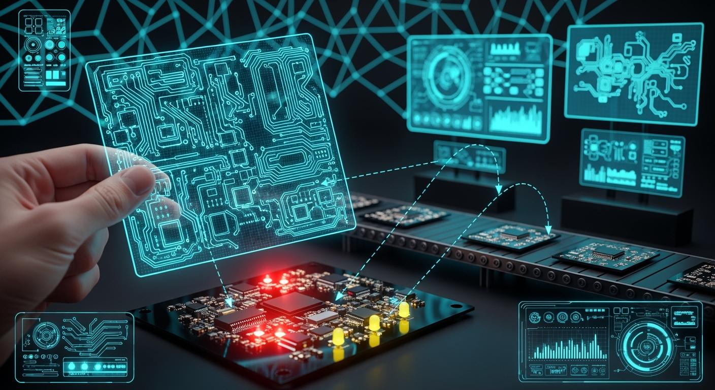
How Gerber Files Guide the PCB Manufacturing Process
When you make a printed circuit board, gerber files are the main plan for building it. These files help machines see your design and make a real board. If you mess up your gerber files, you can have problems like missing board outlines, broken or empty data, or confusing file names. These problems can slow down making your board or cause mistakes in your PCB. To stop these problems, you must check every part of your gerber files. Gerber Files Explained tells you why being exact is important at every step.
Common mistakes include:
Missing board outlines
Missing drill files
Corrupted or empty data
Incorrect file formats
Ambiguous file names
Mismatched design files
Key Takeaways
Gerber files are important blueprints for printed circuit boards. They help guide the making process and make sure boards are made right.
Common mistakes in Gerber files can cause big problems. Missing outlines or wrong formats can make boards bad or slow things down. Always check your files twice.
The RS-274X format makes file handling easier. It puts all needed data in one file. This lowers mistakes compared to the old RS-274D format.
Always check your Gerber files with a viewer before you send them. This helps you find mistakes early and saves time.
Keep your files neat and name them clearly. This helps you talk better with makers and makes the process faster.
Gerber Files Explained
What Is a Gerber File?
Gerber files are like blueprints for your printed circuit board. They show how your digital design becomes a real PCB. These files use ASCII text and vector graphics. You can open them with a simple text editor. You can also share them with anyone in the industry. It is easy to check and change them. This helps you talk to manufacturers and fix mistakes before making the board. Gerber files explained give instructions for each layer, so every part of your PCB is built as you want.
Gerber files explained:
Use ASCII text, so you can read and edit them.
Work on many systems, making them universal.
Give detailed instructions for each PCB layer.
Help you and your manufacturer check designs before making the board.
Gerber files explained are not just computer code. They are the language that connects your design to the machines that build your PCB.
Gerber File Formats
There are two main gerber file formats for making PCBs. The older RS-274D format splits information into different files. You have to add aperture files by hand, which can cause mistakes. The newer RS-274X format puts everything in one file. This makes your work easier and helps you avoid errors. Most new designs use RS-274X because it is flexible and has more features.
Feature | RS-274D | RS-274X |
|---|---|---|
File Structure | Information spread across two files | All information in one file |
Error Risk | More prone to errors due to separate files | Less prone to errors with embedded data |
Aperture File Handling | Requires manual input of aperture files | Aperture files embedded, no manual input |
Flexibility | Limited flexibility | Greater flexibility with advanced features |
Industry Status | Still in use for older designs | Standard format since 1991 |
You need to pick the right gerber file format for your project. If you use RS-274D, you might miss aperture definitions and make mistakes. RS-274X helps you avoid these problems. Gerber file formats have changed to support complex designs and new ways to make PCBs. Now, gerber file formats work with high-density interconnects and flexible PCBs. They also keep up with new technology for making boards.
Why Gerber Files Matter
You use gerber files explained to guide every step of making a PCB. These files have settings, aperture details, XY coordinates, and drawing commands. You use them to make a picture of your PCB. Manufacturers check these files before giving you a price. Gerber files explained help you avoid problems like missing outlines, wrong units, or layers that do not line up.
If you do not use the right gerber file formats, you can have problems. You might miss aperture definitions, have layers that do not match, or use the wrong units. You must export your files in the right format and check them in a viewer. Gerber files explained show you how to fix these problems:
Symptom | Cause | Solution |
|---|---|---|
Missing Aperture Definitions | RS-274D export instead of RS-274X | Re-export using RS-274X format with embedded apertures. |
Layer Misalignment | Inconsistent origin points between files | Use the same origin for all layer exports; verify in a viewer. |
Incorrect Units | Mismatch between export units and expected units | Verify units setting (inches vs. millimeters) and re-export. |
Missing Board Outline | Board outline layer not exported or on wrong layer | Export mechanical layer or board outline as separate file. |
Gerber files explained are the base for turning your design into something you can make. As PCB technology gets better, gerber file formats change to fit new needs. You use them for advanced boards like HDIs and flexible circuits. The industry is also starting to use IPC-2581 for even harder designs. Gerber files explained are still important for clear communication and making boards without mistakes.
Tip: Always check your gerber files explained in a viewer before sending them to your manufacturer. This step helps you catch mistakes early and saves time.
Gerber File Layers and Data
When you prepare a PCB for manufacturing, you need to include several types of gerber data. Each layer in your design has its own gerber file. These files tell the machines exactly what to do. If you work with multi-layer pcbs, you will have more files to manage. You must keep each file organized and named correctly to avoid mistakes.
Copper Layers
Copper layers hold the main electrical paths on your board. You use gerber data to show where the copper traces, pads, and pours go. The top copper layer includes signal traces, component pads, and copper pours. The bottom copper layer does the same for the underside of the PCB. In multi-layer pcbs, you add more copper layers for power and ground planes. The copper layers include:
Traces for electrical connections
Pads for mounting parts
Vias for connecting layers
Copper pours for power and heat control
This gerber data controls how well your PCB works. Good copper layer design means strong signals and safe power delivery.
Solder Mask
The solder mask layer protects your copper from short circuits and helps with soldering. Gerber data for the solder mask shows where to leave openings for pads and where to cover copper. You must check that all solder mask layers line up with the copper pads. Use a gerber viewer to spot misalignment. This step is important for both single-layer and multi-layer pcbs.
Silkscreen
Silkscreen layers use gerber data to print helpful markings on your PCB. These markings include:
Part names like R1 or C2
Polarity marks for diodes and capacitors
Pin 1 indicators for chips
Company logos
Assembly instructions
You need clear silkscreen data for easy assembly and repair.
Drill Data
Drill data tells the machine where to make holes in your PCB. You use this gerber data to set the size and position of each hole. This is important for placing through-hole parts and vias. Accurate drill data keeps your board working right. In multi-layer pcbs, drill data must match all layers to avoid connection problems.
Board Outline
The board outline layer uses gerber data to define the final shape of your PCB. This file tells the machine where to cut the board. The table below shows why the board outline is important:
Layer | Purpose |
|---|---|
Board Outline | Defines the PCB’s physical shape |
Board Outline | Guides cutting to final size |
You must include a clear outline for both simple and multi-layer pcbs. This ensures your board fits in its case and works as planned.
Tip: Always check your gerber data in a viewer before sending it to the manufacturer. This helps you catch errors early and ensures all layers line up.
Using Gerber Files in Manufacturing
Design to Gerber Conversion
You start the pcb fabrication process by turning your design into gerber files. This step is important because it changes your digital layout into instructions that machines can follow. Most engineers use EDA software for this job. You can follow these steps to convert your design:
Schematic Capture: Draw the electrical plan for your pcb.
Component Placement: Put each part in the right spot on the board.
Routing: Draw copper lines to connect the parts.
Design Rule Check (DRC): Make sure your design follows the rules for fabrication.
Gerber File Export: Save each layer as a separate gerber file.
Popular tools like Altium Designer, KiCad, Eagle, and EasyEDA make this process simple. You pick the layers you want, set the units, and export the files. Each tool has its own way to do this, but the goal is the same. You want clear files for every layer of your pcb.
Tip: Always double-check that you include all layers, such as drill and outline files, before moving to the next step in the manufacturing process.
File Preparation and Verification
After you export your gerber files, you need to prepare and check them. This step helps you avoid mistakes in the pcb fabrication process. You use special tools to look at your files and find problems before you send them to the factory.
Here are some common tools you can use:
Tool Name | Functionality |
|---|---|
FreeDFM | Scans gerber files for issues that could stop fabrication. |
Siemens Valor | Checks for errors like wrong trace width or mismatched layers. |
NextPCB Analyzer | Gives you reports and tips for fixing problems in your files. |
You can also use gerber viewers to see your design as it will look after fabrication. These viewers let you zoom in, measure, and check every part. You can catch missing holes, wrong outlines, or layers that do not line up. This step is key in the manufacturing process because it helps you fix problems early.
Gerber viewers help you:
See the real look of your pcb.
Measure parts and check spacing.
Find errors that could cause delays.
Note: Careful file verification can save you time and money in the pcb manufacturing process.
PCB Fabrication Steps
When you finish checking your files, you send them to the factory for the pcb fabrication process. The factory uses your gerber files to guide every machine and worker. Here is how the manufacturing process works:
The factory reads your gerber files and sets up the machines.
The machines print the copper layers on the board.
The factory drills holes using the drill data from your files.
The machines add solder mask and silkscreen layers.
The factory cuts the board to the shape you set in the outline file.
Some factories use your gerber files to make G-code for milling machines. This code tells the machines where to cut and drill. Each step in the pcb fabrication process depends on the accuracy of your files. If you miss a layer or make a mistake, the board may not work.
Tip: Always talk to your factory about their needs before you send your files. This helps you avoid problems in the manufacturing process.
Assembly and Quality Control
After fabrication, your pcb goes to assembly and quality control. The factory uses your gerber files to place parts and check the finished board. Quality teams use these files to inspect every layer and hole. They make sure the board matches your design.
Evidence Description | Source Link |
|---|---|
Gerber files provide detailed instructions for each layer of the PCB, allowing for thorough inspections. | |
Automated inspection tools use gerber files to compare manufactured PCBs against designs. | |
Gerber files are used to verify correct component placement according to design specifications. |
Automated tools check for mistakes like missing parts or wrong traces. These tools compare the finished board to your gerber files. If they find a problem, they stop the process and fix it. This step keeps your pcb manufacturing process smooth and helps you get boards that work.
Tip: Good quality control with gerber files helps you avoid costly errors and keeps your pcb fabrication process on track.
Best Practices for Gerber Files
Organizing and Naming Files
You can stop confusion by keeping your files neat and clear. When you work with printed circuit boards, use standard names for your files. This helps everyone know what each file is for. For example, you can name your files like this:
PCB_Top_Copper.gbr
PCB_Bottom_Copper.gbr
PCB_Top_SolderMask.gbr
PCB_Bottom_SolderMask.gbr
PCB_Drill.gbr
PCB_Outline.gbr
Put your files in folders for each project. Name the folder after your project and version. For big printed circuit board jobs, use subfolders for each part. Write clear descriptions for every file. This helps you and the manufacturer talk better. It also makes making gerber files easier and cuts down on mistakes.
Checking for Errors
Before you send your printed circuit board files to the factory, you must check for mistakes. Many engineers use special tools for this step. One tool is the NextPCB Free Online Gerber Viewer with DFM Check. This tool lets you look at your gerber files and find problems before making the board. It is free and trusted by many engineers. You can spot things like missing layers or wrong spacing. Careful checking helps you avoid delays and keeps your pcb project moving.
Tip: Always use DFM checks in your CAD tool to check trace width, solder mask clearance, and copper-to-edge spacing.
Sharing with Manufacturers
When you send your printed circuit board files to the manufacturer, use names that are easy to read and match your readme. Add a PDF drawing to show the layer stackup, materials, and special notes. Include an assembly drawing for part names and polarity marks. Keep the same origin and units for all layers and drill files. Use RS-274X format with embedded apertures for new designs. Clear communication helps the manufacturer use your gerber files to run CNC machines and lowers mistakes. Standard formats make sure everyone understands your printed circuit board design.
Benefit | How It Helps You |
|---|---|
Gerber files drive CNC equipment | Less human error in production |
Standardized formats | Fewer misunderstandings and mistakes |
Note: Detailed gerber files let manufacturers check your design for manufacturability and help you get high-quality printed circuit boards.
You help make sure PCBs work well when you use Gerber files the right way. Accurate files stop big mistakes, like boards that do not work or projects that take too long. You should always check your files twice and share clear details with your manufacturer.
Mistakes in Gerber files can cause:
Losing money from bad boards
Delays that cost more
Projects that fail and waste time
Knowing Gerber files helps you get:
Manufacturers understand your files everywhere
Better teamwork and faster work
More efficient production
Common Communication Issue | Description |
|---|---|
Design Mismatch | The finished board is not what you wanted |
Incomplete Files | Missing info leads to errors in making boards |
Unorganized File Labels | Confusing names make the process slower |
You can stop these problems by checking your files and keeping your communication simple. This saves money and helps you get the best PCBs for your projects.
FAQ
What is a Gerber drawing file?
A gerber drawing file gives machines the instructions to build your circuit board. You use it to show where copper, solder mask, and silkscreen go. This file helps you turn your digital design into a real board during pcb design and manufacturing.
How do I check my Gerber files before sending them to a manufacturer?
You should use a viewer to open and inspect each layer. A gerber viewer application lets you see your design as the factory will. You can spot missing holes, wrong outlines, or misaligned layers with a viewer.
Why do I need to use a viewer for my Gerber files?
A viewer helps you catch mistakes before production. You can check if all layers line up and if the board outline is correct. Using a viewer saves you time and money by preventing errors.
Can I use a viewer on any computer?
Yes, you can use a viewer on most computers. Many free viewers work on Windows, Mac, and Linux. You only need to download the viewer and open your files to start checking your design.
What should I do if my viewer shows an error?
If your viewer finds a problem, fix your design in your CAD tool. Export the files again and check them with the viewer. Repeat this until the viewer shows your board is ready for manufacturing.
See Also
An In-Depth Overview of PCBA Manufacturing for All Levels
Essential Tips for BOM Sourcing in PCBA Projects
Navigating Component Procurement for Effective PCBA Production
Design Strategies for Industrial Controller Printed Circuit Boards