PCBA for POS Systems and Payment Terminals
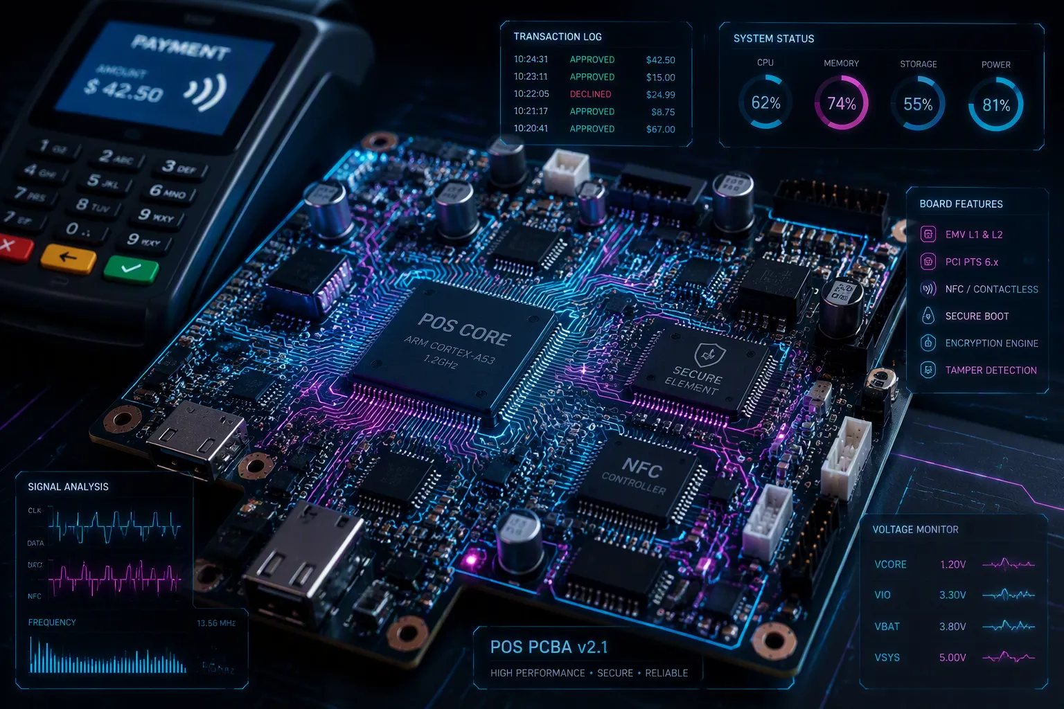
You might wonder what makes pcba for pos systems different from standard electronics. The answer is the board's complexity. A single PCB holds an EMV contact reader, an NFC front end, a secure element, a PIN pad, and an application processor. Each part needs careful placement to stop interference.
Security shapes every design choice. Payment processing systems always face threats from physical tampering and data theft. Unlike consumer devices, point-of-sale terminals must meet strict rules. Your payment pos system needs hardware-level encryption and tamper detection.
Reliability is just as important. If a terminal fails, it causes lost sales and unhappy customers. Mobile payment devices add limits on power and heat problems. Every choice, from picking parts to routing traces, affects performance and safety. This introduction gets you ready to learn about design, security, connectivity, and manufacturing challenges ahead.
Key Takeaways
Secure your POS board with anti-tamper mesh and secure elements to protect encryption keys and meet PCI-PTS standards.
To make your NFC and EMV work well, design your PCB with careful component placement and trace routing.
Balance the power and heat in your POS terminal to keep it working well and stop tamper detection from failing.
Support different connections like NFC, Wi-Fi, and Ethernet for many payment methods.
Work with a skilled manufacturer to handle certifications and make your design easier to produce.
Designing PCBA for POS Systems: Core Hardware Challenges
Integrating Essential Payment Components
Your pos board combines five critical parts. The EMV contact reader processes chip card data. The NFC front end handles contactless payments. A secure element stores encryption keys. The PIN pad captures user input. An application processor runs the software stack. The pos system depends on each component working correctly.
Each component needs careful placement. Consider the NFC antenna design. You must maintain 1mm clearance between the antenna and ground plane. This prevents eddy currents that weaken the magnetic field. Keep high-speed digital traces at least 10mm from the antenna. This isolation stops noise coupling at 13.56MHz. Your pos design must follow these rules.
Trace geometry affects signal integrity. Use 45° corners instead of sharp bends. Route parallel traces for consistent inductance. Set trace width to 0.2mm with 0.02mm tolerance. Validate impedance with a network analyzer. These steps ensure reliable pos communication.
Choose your PCB material carefully. FR4 works for standard designs. Flex circuits fit compact mobile devices. Ceramic substrates handle high-frequency needs. Symmetrical coil designs ensure uniform field distribution. Your pos board material choice affects performance.
The NFC module offers advanced features. Automatic antenna tuning with variable capacitors simplifies matching. Dynamic Power Control manages RF output without host MCU load. This helps meet EMVCo 3.2 compliance. Dual antenna support gives layout flexibility. The module resists TFT display noise. Internal RF debugging via AUX outputs supports PCI-compliant design.
A secure microcontroller manages tamper detection. It monitors the anti-tamper mesh for breaches. It verifies the secure element's integrity. Your payment processing systems depend on this hardware security. The tamper detection circuit must respond instantly.
Managing Power and Thermal Constraints
Power consumption affects your pos design directly. The display uses 500 mW active and 50 mW standby. The card reader draws 200 mW continuously. Your system may reach 5 W in active mode. The industry average is 3 W. Your target should be 3 W active and 0.5 W standby. Your pos terminal must meet these targets.
Thermal management matters with these loads. The application processor generates heat. The NFC front end adds thermal load. The PIN pad backlight contributes heat. Without dissipation, components degrade. The secure microcontroller operates best at lower temperatures. Tamper detection circuits must stay within range. Extreme heat can trigger false tamper events.
Your pos terminal must balance power and heat. Choose efficient power management ICs. Use low-power display technologies. Optimize firmware for low-power states. These choices reduce load on your payment processing systems. The pos system must switch between states smoothly.
The challenge is significant. Your pcba for pos systems must handle multiple states. Active mode draws full power. Standby mode conserves energy. Smooth transitions prevent transaction corruption. Your payment processing systems rely on this stability. Your pcba for pos systems must pass all compliance tests.
Security-First PCBA for Payment Processing Systems
Implementing Anti-Tamper and Secure Elements
Your pos board faces real danger from people who try to break it. They might drill, cut, or probe the board to steal secret data. You need strong protection at the hardware level. Anti-tamper mesh is the first shield against these attacks.
Anti-tamper mesh is a network of tiny wires on the PCB. These wires carry steady electrical signals. The system watches for changes in resistance or capacitance. Any change means something is wrong. Drilling through the board changes the wire resistance. Cutting a wire breaks the circuit. The tamper detection system reacts right away.
When the mesh detects a break, the secure microcontroller acts fast. It wipes secret encryption keys from memory. It may also short the microcontroller's power to ground. This stops data theft even if the attacker keeps going. Your payment processing systems depend on this quick response.
Advanced systems use a flexible printed circuit mesh with rubber-like epoxy. The epoxy tears the conductive ink from the foil when someone disturbs it. This combo makes physical attacks very hard. Ingenico payment terminals use this method successfully. The tamper-detecting shell has not been publicly broken yet.
Secure elements add another layer of safety. These special chips store encryption keys and do sensitive work. They keep important data away from the main application processor. Even if the main processor is hacked, the secure element's data stays safe.
Secure elements can pass tough security tests, like Common Criteria. These tests prove that the secure element really protects as promised. Outside experts check and verify the security. Your pos design should use certified secure elements.
The certification system has many levels. Payment apps need VISA Chip Security Program or MasterCard CAST approval. The platform operating system needs GlobalPlatform SE Configuration certification. Hardware and firmware must pass EMVCo IC Security Evaluation. Each level adds trust to your payment processing systems.
Ensuring Data Encryption and Key Protection
Encryption keeps transaction data safe during the payment process. Your pos board must use strong math codes to scramble data. These codes mix up the data so no one else can read it. The encrypted keypad module captures PIN entries safely. It encrypts the data before sending it to the application processor.
Safe key storage is the base of your security plan. Keys must never be unencrypted outside a protected area. Hardware Security Modules (HSMs) create, store, and protect encryption keys. These special devices keep master keys inside a tamper-proof box. Clear keys are never exposed to other services.
Key management follows a clear process. First, encryption keys are created inside tamper-proof HSMs. Keys never leave the HSM unencrypted. Second, keys are moved using encrypted channels with key encryption keys. Dual control and split knowledge rules stop any single person from getting a full key. Third, certified injection equipment puts keys into payment terminals in a PCI-certified facility. Trained workers do this job under controlled conditions.
Your pos board must support remote key injection and key lifecycle management. An HSM can create or derive terminal keys. It protects the master material and wraps keys for safe transport. Auditable, dual-control workflows keep everything accountable.
Secure memory technologies protect keys when not in use. These special memory cells resist probing and side-channel attacks. They detect voltage changes and temperature extremes. The secure microcontroller checks the stored keys' integrity before each transaction. This check ensures every transaction is safe.
Your payment processing systems must meet PCI-PTS security standards. These rules require secure boot processes and encrypted communication. They demand tamper resistance and strict security testing. Each POS device must prove it can resist hacking. The terminal must protect sensitive information at all times.
Hardware-level encryption and secure key management work together. They create a defense-in-depth strategy that protects your POS system from physical and logical attacks. Your payment processing systems get stronger through this layered approach.
Connectivity Options for Modern Payment Terminals
Supporting Contact and Contactless Interfaces
Your pos terminal handles many payment methods. Customers can use magnetic stripe cards, EMV chip cards, or contactless payments. Each method needs different hardware on your pos board.
The EMV contact reader reads chip card data. The magstripe reader handles older cards. Both readers need careful placement on your pos board to avoid interference.
The nfc interface handles contactless transactions. The nfc antenna needs a flat coil with 3-6 turns. Trace width should be 1-5 mm with spacing of 0.25-1 mm. Use 2 oz copper to cut losses. Coil diameter should be 25-70 mm for best results. Match antenna impedance to the nfc chip input. Use a capacitor and inductor network to reduce signal reflection. Fine-tune nfc resonance to 13.56 MHz using NP0 or C0G ceramic capacitors.
Put a ground plane under the nfc antenna. Add shielding cans to block noise. Include filters and ferrite beads for EMI suppression. Use RF simulation tools to check performance. Build and test prototypes before mass production.
For your pos design, use a modular setup. Place the nfc antenna and matching network on a separate PCB. Keep the nfc controller on the main device PCB. This design gives you flexibility in controller choice. It also makes production easier.
Your payment processing systems must support all these interfaces. The pos board must switch between contact and contactless modes smoothly.
Enabling Wireless and Wired Communication
Your pos terminal needs reliable links to payment networks. Countertop terminals often use Ethernet or USB. Mobile payment devices need Wi-Fi or Bluetooth. Smart terminals may combine several options.
Ethernet gives stable connections for fixed terminals. USB offers flexibility for peripherals. Both work well for countertop pos systems.
Wi-Fi enables wireless connections in stores. Your pos terminal can connect without cables. Bluetooth supports links to smartphones and tablets.
Your nfc module handles close-range wireless data exchange. The system works with the contactless interface. Together they enable secure transactions. The nfc front end must meet EMVCo 3.2 compliance.
Your payment processing systems depend on reliable connectivity. The pos terminal must keep stable connections during transactions. Any interruption can cause failures. Your pos design must include strong communication hardware.
Wired connections offer security and reliability. Ethernet provides encrypted data transfer. USB connections support secure peripherals. Wireless options need strong encryption. Your pos board must support both options.
The nfc antenna and matching network need careful design. Use FR4 or Rogers 4350B substrate material. Choose 1-2 oz copper layers. Keep precise impedance control. Prefer ENIG or immersion silver surface finish.
Your payment processing systems must handle all connectivity types. The device must switch between modes automatically.
Manufacturing and Compliance for Payment PCBA
Navigating Certifications and Standards
Your payment terminal must pass several certifications before it can be sold. Each one checks a different part of your design. You cannot skip any of them. The list includes:
PCI-PTS 6.x: This rule covers PIN transaction safety. It checks your tamper detection and secure key storage.
EMV L1+L2: These levels check the chip card interface and payment app functions.
GMS: The GlobalPlatform certification makes sure secure element management works.
FCC: This covers electromagnetic interference in the United States.
CE: This mark shows the device meets European safety and health rules.
RoHS 3.0: This rule limits dangerous substances in your manufacturing process.
Your pci-pts compliance needs shape your whole design plan. The rule demands physical tamper resistance. It requires secure boot processes. It requires encrypted communication channels. Your board must show it can resist hacking. Your tamper detection must react right away to any break-in.
These certifications affect your manufacturing timeline. Each test takes time. Each failure means redesign and retesting. You should plan for several rounds of certification testing. Your manufacturing partner should know these requirements well.
Optimizing DFM and Reducing BOM Costs
High-mix, low-volume production creates unique challenges for your pos manufacturing. You might build several board versions in small amounts. Each version needs different parts and test steps. Common risks include:
Wrong revision builds
BOM mismatches
Setup errors
Missing or wrong parts
Incomplete work instructions
Inconsistent inspection rules
Test procedure confusion
Delayed material availability
Poor configuration control
Rework from unclear requirements
You can lower these risks with careful design for manufacturability. Your pcba for pos systems should follow proven DFM rules. Component spacing stops solder bridging. Consistent orientation reduces placement errors. Test point access speeds up quality checks.
Follow these specific DFM guidelines for your pos board:
Keep annular ring >3.5 mils for vias and >6 mils for through-hole pins
Add teardrops to traces to stop connection breakage
Use minimum trace width and spacing of 6 mils
Include fiducial markers for automated assembly alignment
Avoid acute angles in traces to stop chemical trapping
Use standard component sizes like 0603 or 0805
Minimize layer count to reduce complexity
Set realistic tolerances around ±10%
Clear silkscreen markings with minimum text height of 0.8mm
Your payment processing systems depend on reliable manufacturing. Each defect costs money and time. Each rework adds new risks. Your tamper detection circuits must work perfectly after assembly. Your encryption hardware must work without errors. Your tamper mesh must detect any physical break-in. Your tamper response must erase keys right away. Your tamper sensors must cover every weak spot. Your tamper monitoring must run all the time. Your tamper alerts must trigger instant action.
Configuration control matters for your pos production. You must track multiple active board types. You must manage options and revisions without mixing materials. Your documentation must stay current. Your operators should not rely on memory.
Material management brings another challenge. Fragmented inventory complicates your supply chain. You must separate common parts from product-specific ones. You must manage minimum order amounts. You must handle old stock carefully.
Changeover management affects your efficiency. Switching between products can cause errors. Your team must follow clear steps. Your test programs must match specific board revisions. Your inspection rules must adapt across assemblies.
Your payment processing systems need steady quality. Your pos terminal must meet every spec. Your tamper detection circuits must react instantly. Your cryptography must protect every transaction. Your secure key storage must stay safe. Your detection systems must catch every problem. Your detection methods must stay ahead of attackers. Your detection accuracy sets your security level.
Working with an experienced manufacturing partner helps you handle these challenges. They understand the certification process. They know how to optimize your pos design for production. They can cut your time-to-market and lower your costs. Your payment processing systems will reach customers faster and work reliably.
Your payment terminal needs careful work in design, security, connections, and rules. It is not a one-size-fits-all device. The parts you pick and the company you work with decide if you succeed. You need a partner who knows your payment systems well. They must be good at DFM, building security, and getting certifications. Your tamper detection circuits must work without errors. Your tamper response must erase keys right away. Your tamper mesh must cover all weak spots. Your tamper sensors must watch all the time. An experienced manufacturer gets your product to market faster and cuts down risks. Your PCBA for POS systems will reach customers sooner. Your POS device must pass all standards. Your payment processing systems will work well every time.
FAQ
Why does NFC antenna placement matter so much on a POS board?
NFC antenna placement directly affects how well transactions work. You need at least 1mm of space between the antenna and the ground plane. Keep high-speed digital traces 10mm away from the antenna. Bad placement causes weak signals and failed contactless payments.
What happens when tamper detection triggers?
The secure microcontroller wipes all encryption keys from memory right away. It may also short the microcontroller's power to ground. This response stops attackers from stealing sensitive data. Your payment processing systems stay safe even during physical attacks.
How long does certification testing take?
Certification timelines vary based on how complex your design is. PCI-PTS, EMVCo, and FCC testing each need separate evaluation cycles. Plan for multiple rounds of testing. Each failure means redesign and retesting. Work with an experienced manufacturing partner to make this process smoother.
Can I use standard FR4 material for my payment terminal PCB?
Yes, FR4 works for most countertop terminals. Flex circuits suit compact mobile devices. Ceramic substrates handle high-frequency needs. Your material choice depends on your form factor and performance needs. Think about thermal demands and signal integrity when choosing.
What is the most common manufacturing mistake for POS boards?
Configuration control errors cause most production issues. Wrong board revisions, BOM mismatches, and setup errors create costly rework. You must track multiple active board types carefully. Clear documentation and consistent inspection rules prevent these problems.
See Also
Understanding PCBA and Its Essential Components
Decoding the Meaning of PCBA in Electronics
PCBA Processing Demands for Medical Equipment Manufacturing
The Role of Industrial Serial Screen PCBA in Modern Industry
Sourcing Electronic Components for PCBA Production Processes
