PCB pad design guidelines for robotic and automated soldering

High-volume pcb assembly production often encounters costly solder defects like tombstoning and bridging. These issues increase rework costs and field failures. Have you experienced such problems? Following pcb pad design guidelines is your primary lever for zero-defect robotic soldering. This article covers geometry, thermal management, finishes, and process control, all grounded in IPC J-STD-001. The outcome is reliable, repeatable, and inspectable solder joints in automated environments. You achieve consistent quality and efficiency through these methods. Robotic soldering automation requires careful attention to these guidelines. Automated soldering solutions also depend on proper pad design for pcb soldering. Production methods improve with consistent joint consistency. Repeatability ensures high-quality results.
Key Takeaways
Pad design is a strategic investment in manufacturing yield, not just a layout task.
Use IPC-7351 standards to calculate pad dimensions for reliable robotic soldering.
Thermal relief patterns prevent cold solder joints by balancing heat flow and conductivity.
NSMD pads offer better reliability for fine-pitch components under 0.65 mm pitch.
ENIG finish provides superior wetting and planarity for automated soldering.
Design pads with symmetric geometry and adequate spacing to prevent bridging and tombstoning.
Fill and cap vias-in-pad to prevent solder wicking and ensure joint strength.
Matte finishes and clear fiducials improve AOI accuracy and reduce false defects.
Fundamentals of Automated Soldering for PCB Assembly
Automated systems demand precise process windows that manual soldering stations simply do not require. A human operator can adapt to slight variations in pad geometry or heat distribution. A robot cannot. It follows the programmed path exactly, every time. This precision makes pad design critical for successful automation. IPC J-STD-001 provides acceptance criteria for voids, wetting, and other quality factors that your pad design must support from the start.
Reflow, Wave, and Selective Soldering Differences
Each soldering method exposes your PCB to heat differently. This variation directly affects how you design your pads.
Heat Exposure and Pad Stress Variations
Reflow soldering heats the entire board gradually. The thermal profile moves through preheat, soak, reflow, and cooling stages. Peak temperatures reach 220-260°C. The board experiences this heat for 30-90 seconds. Wave soldering applies heat only to the bottom side. The board contacts molten solder at 250-260°C for just a few seconds. This rapid spike creates thermal shock. Selective soldering sits between these extremes. It targets specific areas with a localized solder wave or iron.
Parameter | Wave Soldering | Reflow Soldering |
|---|---|---|
Peak Temperature | ~250-270°C | ~220-250°C |
Heating Method | Direct contact with molten solder wave | Controlled oven heating (convection/infrared) |
Typical Duration at Peak | Short contact time (seconds) | 30-90 seconds |
Primary Component Type | Through-hole (THT) | Surface-mount (SMT) |
Thermal Profile Shape | Rapid spike and cool | Gradual ramp, soak, reflow, cool |
These differences matter because your pads must survive the thermal stress. Wave soldering pads need robustness against sudden temperature spikes. Reflow pads require thermal relief to prevent heat from conducting away too quickly.
Process-Specific Pad Geometry Requirements
Reflow soldering requires balanced pad geometry, proper solder mask clearance, and optimized thermal relief. Selective soldering imposes stricter geometric constraints. Per IPC-7251, you need specific dimensions for reliable robotic assembly.
Pad Geometry Parameter | Selective Soldering Requirement (per IPC-7251) |
|---|---|
Annular Ring Width | 0.15 mm – 0.25 mm |
Solder Mask Expansion | 0.1 mm – 0.15 mm at pad edges |
Via Spacing from Pad | Minimum 1.5–2 mm (to prevent solder thieving) |
Thermal Relief Spokes | 0.3–0.5 mm spoke widths (mandatory) |
You must also consider component spacing and directional layout for wave soldering. Adequate pad-to-pad distance prevents bridging. Hole size tolerance ensures proper solder flow for through-hole components.
Process Control Parameters for Robotic Soldering
Robotic soldering cells bring their own set of control parameters. You must understand how each one interacts with your pad design.
Solder Feed, Iron Angle, and Dwell Time
Your robotic soldering system feeds solder wire at a controlled rate. The iron angle determines how solder wets the pad. Dwell time controls heat transfer. These parameters work together. If your pad geometry does not match the programmed feed rate, you get irregular deposits. If the iron angle does not align with the pad surface, wetting suffers. You must tune these variables for each pad design in your assembly.
Fixture Repeatability and Its Impact on Pad Alignment
Your fixture holds the PCB in place during soldering. Its repeatability directly affects alignment accuracy.
If the fixture locates the part differently each time, the robot may still move perfectly but dispense in the wrong place relative to the product. That means the motion system can be correct while the real output is still inaccurate.
Even small deviations in XYZ positioning can produce variable heat transfer, irregular solder deposits, or missed joints altogether. Fixture wear can introduce drift over time.
You must design pads with enough tolerance to accommodate minor fixture variations. This approach ensures joint consistency even when the fixture shifts slightly between cycles.
PCB Pad Design Guidelines for Pad Size and Spacing
The dimensions you choose for your pads determine whether your automated soldering process succeeds. Incorrect sizing leads to poor fillets, bridging, or weak joints. Following proper pcb pad design guidelines for your robotic soldering system ensures reliable results. This section gives you the specific formulas and rules you need for your automated assembly.
Calculating Pad Dimensions for Standard Components
You must calculate pad dimensions based on component lead geometry and the required solder fillet. The IPC-7351 standard provides the equations you need for your design.
Toe, Heel, and Side Fillet Requirements
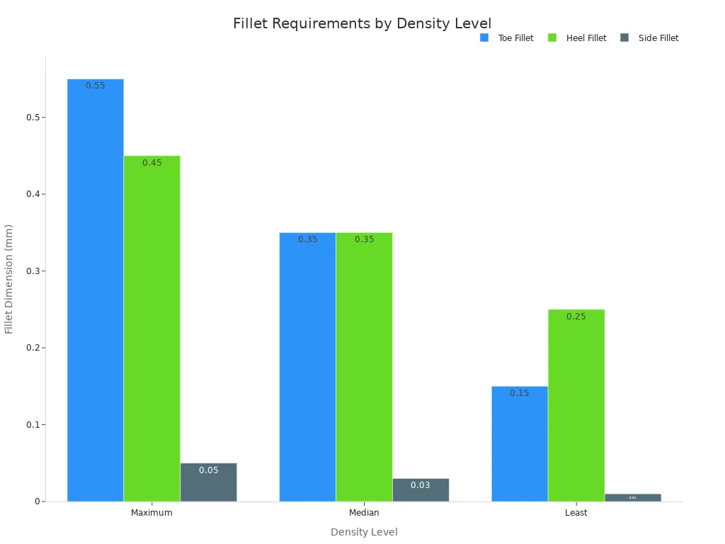
Three solder fillet values control your pad dimensions: the toe fillet (Jt), heel fillet (Jh), and side fillet (Js). The IPC-7351 standard specifies three equations:
Zmax = Lmin + 2Jt + sqrt(Cl²+F²+P²)
Gmin = Smax – 2Jh – sqrt(Cs²+F²+P²)
Xmax = Wmin + 2Js + sqrt(Cw²+F²+P²)
In these equations, Jt, Jh, and Js represent the solder fillet values. You add or subtract these values from the component dimensions to determine the final pad size. The fillet values change based on your chosen density level.
Density Level | Toe Fillet (Jt) | Heel Fillet (Jh) | Side Fillet (Js) |
|---|---|---|---|
Maximum | 0.55 mm | 0.45 mm | 0.05 mm |
Median | 0.35 mm | 0.35 mm | 0.03 mm |
Least | 0.15 mm | 0.25 mm | 0.01 mm |
For example, a larger toe fillet in the Maximum density level directly increases the pad length. A smaller side fillet results in a narrower pad. Your choice of density level directly alters the calculated pad dimensions.
Using IPC-7351 Standards as a Baseline
Use IPC-7351 as your starting point for all pad dimensions. The standard accounts for manufacturing tolerances, component variations, and placement accuracy. For robotic soldering, the Median density level works well. It provides enough fillet volume for reliable joints while maintaining reasonable component spacing. These pcb pad design guidelines apply to any automated soldering method you choose.
Through-Hole Pad Design for Robotic Assembly
Through-hole components require different pad design rules. You must account for the pin diameter, hole clearance, and annular ring width.
Sizing Pads Based on Pin Diameter and Hole Clearance
The hole size determines how solder flows into the joint. For non-circular pins, calculate the maximum effective diameter first. For a square or rectangular pin, use the diagonal:
Maximum effective diameter = √(a² + b²)
For a 0.64 mm × 0.64 mm pin, the effective diameter is √(0.64² + 0.64²) = 0.905 mm. Then, the hole diameter = 0.905 mm + 0.2 mm = 1.1 mm.
The pad diameter formula follows:
Pad Diameter = Hole Diameter + 2 × (Minimum Annular Ring Width) + (Manufacturing Tolerance)
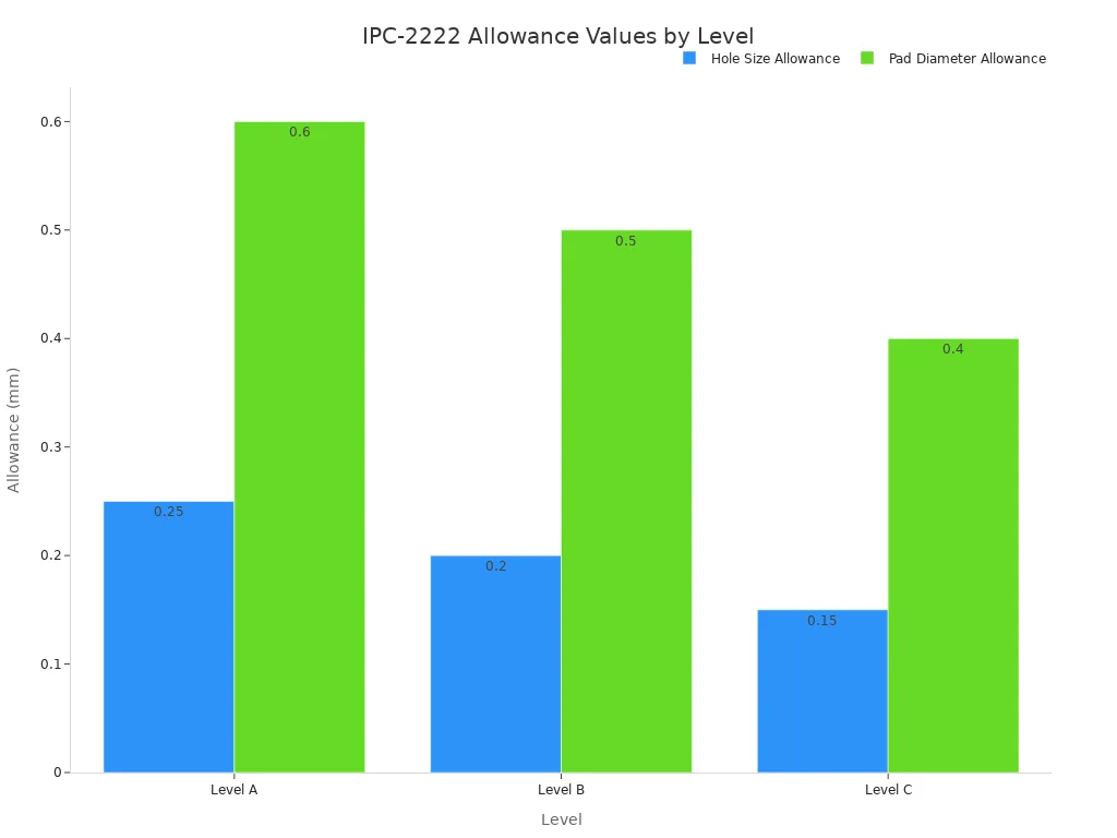
IPC-2222 specifies different allowances based on your product class:
Step | Formula (per IPC-2222/2221) | Level A | Level B | Level C |
|---|---|---|---|---|
1. Minimum hole size | Max lead diameter + allowance | +0.25 mm | +0.20 mm | +0.15 mm |
2. Pad diameter | Minimum hole size + 0.1 mm (2× annular ring) + fabrication allowance | +0.60 mm | +0.50 mm | +0.40 mm |
Note that the minimum annular ring is 0.05 mm (50 µm) per IPC-2221.
Hole clearance affects solder fill quality. A hole diameter of 0.25 mm to 0.40 mm larger than the lead diameter is optimal. If the clearance is too tight, solder will not flow into the joint. If the clearance is too loose, the mechanical strength weakens. Ensure the pin diameter is at least 60% of the hole size for proper wicking. This balance is critical for your robotic soldering setup.
Annular Ring Requirements for Mechanical Strength
To withstand soldering stress and insertion forces, annular ring width should be 0.20 mm or larger. This applies to robotic soldering where consistent mechanical strength is critical. A smaller ring will fail under automated handling. The annular ring provides the mechanical connection between the pad and the board. You should verify the ring width during your design review.
Managing Pad-to-Pad Spacing to Prevent Bridging
Bridging is a common defect in automated soldering. You prevent it by controlling the pad spacing between pads.
Minimum Spacing for Fine-Pitch Components
For fine-pitch components, the spacing between pads must be carefully calculated. The tighter the pitch, the higher the risk of bridging. Follow the IPC-7351 recommendations for each component type. Generally, you want at least 0.20 mm of space between adjacent pads for robotic soldering. Your automated systems may require more clearance than manual soldering because the robot cannot adapt its path mid-cycle. Proper pad spacing prevents many defects and improves your production yield.
Solder Mask Webbing and Its Role in Isolation
Solder mask webbing acts as a barrier between pads. It prevents solder from bridging during the soldering process. Design the solder mask to cover the space between pads completely. This creates a physical barrier that stops solder from flowing across the gap. The mask also provides electrical isolation between adjacent pads. For automated processes, you need consistent mask coverage to ensure repeatable results. The combination of correct pad spacing and mask webbing gives you reliable joint consistency. Without proper webbing, even correctly sized pads can bridge during automated soldering. You should include this check in your design rules.
Thermal Relief and Heat Management for Robotic Soldering
Heat management is a critical factor in automated soldering solutions. When you connect a pad to a large copper plane, you create a heat sink. This heat sink steals thermal energy from the joint. You need the right thermal relief to maintain consistent quality.
The Problem with Solid Copper Planes
A solid copper plane draws heat away from the soldering iron rapidly. The iron cannot supply heat fast enough. The joint never achieves proper wetting.
Cold Solder Joints and Insufficient Wetting
Ground pins connected to large copper planes act as massive heat sinks. Without thermal relief patterns, the copper plane pulls heat away faster than you can apply it. The joint fails to reach the temperature needed for wetting. This condition produces cold solder joints.
In automated production, a poorly tuned reflow oven creates the same problem. Large thermal lands or ground planes prevent the alloy from reaching the required temperature. The result is insufficient wetting and weak joints.
You must remember that lands are only held to the substrate with glue. Excessive heat or poor thermal relief can cause lifting. You lose the land entirely. This is a catastrophic failure in any pcb assembly line.
Designing Effective Thermal Relief Patterns
Thermal relief patterns are essential for soldering automation and production success. They provide repeatability across every cycle. They create a thermal barrier between the land and the copper plane. This barrier allows the land to reach the required temperature for proper wetting.
Spoke Width, Number, and Placement
The spoke width and number determine heat flow. You must balance heat during the process with electrical conductivity.
IPC-2221B sets a minimum spoke width of 0.2 mm (8 mil). Four spokes is the normal maximum. The table below shows recommended dimensions for different component classes.
Component Class | Spoke Width (mm/mil) | Air Gap (mm/mil) |
|---|---|---|
Fine-pitch passives (0402, 0603) | 0.10–0.20 / 4–8 | 0.20–0.30 / 8–12 |
General SMD (0805, SOT-23, SOIC) | 0.20–0.30 / 8–12 | 0.25–0.40 / 10–16 |
Through-hole pins on a plane | 0.30–0.50 / 12–20 | 0.40–0.60 / 16–24 |
Any pad above 3 A continuous | None (direct connect) | Not applicable |
For fine-pitch components, use the narrower spoke widths. The smaller air gap provides enough thermal isolation. For larger components and through-hole pins, wider spokes improve current capacity.
Balancing Electrical Conductivity and Heat Flow
You must balance two competing requirements. More spokes improve electrical conductivity. They also increase heat flow away from the land. Fewer spokes reduce heat loss. They also increase electrical resistance.
The key is to match the thermal relief to your specific design. Components carrying high current need direct connections. Lower current designs can use narrower spokes. Your robotic soldering setup benefits from the right balance.
Vias-in-Pad and Thermal Management
Vias placed directly in lands create challenges for pcb soldering. They also create a wicking path for the molten alloy. During the joint formation, the material can flow down the via hole. This leaves the joint starved.
Filled and Capped Vias for Solder Wicking Prevention
To prevent solder from wicking down the via, you fill the hole with epoxy and cap it with copper plating. The plating stops the alloy from migrating down the land. The arrangement maintains electrical and thermal conductivity.
The epoxy fill adds mechanical strength. It maintains flatness of the land. It protects against damage from trapped air expanding during reflow. You should use an epoxy with high thermal conductivity. The copper plating offers enough current-carrying capability.
IPC-4761 describes several methods for via protection:
Via Plugging: Non-conductive epoxy filling prevents the alloy from entering the via. It maintains structural integrity. This method works well for high-density designs with BGAs.
Via Tenting: Tenting can be applied on one or both sides of the board. It is cost-effective for less complex boards. It prevents the alloy from wicking by sealing the via entrance.
Optimized Solder Mask Design: IPC-SM-840 provides guidelines for automated systems. Engineers should design masks to cover via edges while leaving sufficient land area.
Designers should limit tenting to vias under 0.3 mm diameter. The annular ring width should be at least 0.15 mm. This ensures tent bridging without pinholes.
Fabrication notes must specify LPI mask thickness around 15-25 microns. They must also specify the tenting sides. Align these requirements with IPC-4761.
For plugging, select non-conductive fill for signal integrity preservation. Target 100% fill verified by automated X-ray inspection. Process controls include pre-bake to remove moisture and post-cure for filler stability.
These pcb pad design guidelines help you achieve reliable thermal management in your automated assembly. You create consistent joints with fewer defects. This approach improves joint consistency across every board. Your robotic soldering process produces high-quality results every cycle.
Solder Mask and Finish Selection for Reliable Soldering
The solder mask and surface finish you choose directly affect the quality of your automated soldering process. These choices determine how well the solder wets the pad and how consistently your robotic system forms joints. You must align these decisions with IPC J-STD-001 criteria for acceptable wetting and void levels. Proper design rules also enforce adequate pad-to-trace clearance to avoid mask slivers.
Solder Mask Design for Automated Processes
Your solder mask design controls the exposed copper area and prevents solder from flowing where it does not belong. For automated systems, the mask must be precise and repeatable.
Solder Mask Defined (SMD) vs. Non-Solder Mask Defined (NSMD) Pads
The choice between SMD and NSMD pads affects your solder joint reliability. For pitches below 0.65 mm, NSMD pads are frequently preferred to maximize joint robustness. Larger pitch components may use SMD pads when board space is tight. Applications with repeated temperature excursions benefit from the stress distribution advantages of NSMD geometry.
Reliability Factor | Solder Mask Defined (SMD) | Non-Solder Mask Defined (NSMD) |
|---|---|---|
Solder joint strength | Solder restricted to mask opening; mechanical anchoring is stronger, reducing pad lift risk | Solder wets top and sides of copper pad, forming stronger joints with better stress distribution |
Thermal cycling performance | Higher risk of stress concentration at mask edge | Preferred for high thermal cycling demands due to even stress distribution |
Solder voiding risk | High | Low |
Sensitivity to mask misalignment | High - requires precise alignment to ensure correct pad exposure | Low - copper defines pad boundary, leaving more margin for alignment error |
Solder ball defects | Higher risk if paste lands on mask due to misalignment | Reduced risk of random solder balls due to larger mask opening |
For your robotic soldering process, NSMD pads generally offer better consistency and reliability. Use SMD pads only when board real estate is constrained and pitch is larger than 0.65 mm.
Solder Mask Slivers and Clearance Rules
The minimum dimension for solder mask dams must be 0.1 mm (4 mil) to prevent solder bridging and create insulated areas. This value is a hard minimum for all applications, including fine-pitch components.
Component Category | Pitch | Minimum Solder Mask Dam |
|---|---|---|
Fine-pitch ICs | <0.65 mm | ≥3–4 mil |
Very fine-pitch ICs | <0.5 mm | ≥3 mil |
Fine-pitch BGA | <0.5 mm | ≥2–3 mil |
Fine-pitch connectors | <1.0 mm | ≥4 mil |
Small discrete components | - | ≥3–4 mil |
These values prevent solder mask slivers and ensure manufacturability. You must enforce these rules in your design to avoid pad spacing issues that cause bridging in automated assembly.
Choosing the Right Surface Finish
The surface finish on your pads determines solderability and shelf life. For robotic soldering, you need a finish that provides consistent wetting across every board.
HASL vs. ENIG vs. OSP for Robotic Soldering
Finish | Shelf Life | Solderability for Robotic Soldering | Planarity | Cost |
|---|---|---|---|---|
HASL | Exceeds 12 months, durable even in less-than-ideal storage | Excellent; strong bonding, preferred for through-hole components | Poor; uneven surface (1-5 micrometers variation) can cause issues with fine-pitch SMT | Affordable |
ENIG | Exceeds 24 months; resists corrosion and oxidation | Superior; excellent wetting, handles multiple reflow cycles without degrading | Excellent; consistent finish with gold thickness control (0.05-0.1 micrometers) | Significantly more expensive |
OSP | 6-12 months under proper storage (below 25°C, below 60% humidity) | Effective for a single cycle; may struggle after first soldering attempt if not stored properly; not ideal for multiple reflows | Excellent; flat surface suitable for fine-pitch SMT | Low cost |
For high-volume automated soldering, ENIG provides the best balance of reliability and planarity. Your soldering solutions benefit from its consistent wetting. OSP is a low-cost option if you control storage conditions carefully. HASL works well for through-hole components but may cause issues with fine-pitch SMT due to its uneven surface.
The Effect of Finish on Solder Joint Reliability and Shelf Life
ENIG supports multiple reflow cycles without degrading, which is critical for complex boards. OSP requires strict storage control to maintain solderability. HASL offers excellent bonding for through-hole components but may not meet flatness requirements for fine-pitch pads. You must match the finish to your production needs and expected shelf life.
Solder Wire and Material Selection for Robotic Systems
The solder wire you feed into your robotic system must have consistent characteristics. Variations in diameter or alloy composition cause defects.
Corded Wire Characteristics for Consistent Feed
Your robotic system requires solder wire with a consistent diameter and minimal flux spattering. Corded wire designed for automated feed must have a uniform outer diameter. Premature flux release can cause voids and weak joints. You should select wire with a flux core that activates at the correct temperature for your process.
Reducing Spattering and Enhancing Joint Quality
Spattering creates solder balls that cause bridging and contamination. To reduce spattering, use wire with a flux that has low volatility. Keep the iron tip clean and at the correct temperature. The dwell time must be long enough to allow complete wetting but short enough to avoid overheating the flux. Proper material selection and process control produce high-quality joints with each cycle.
Your choice of solder mask, finish, and wire determines the success of your robotic soldering process. These decisions affect the quality of every joint. You must align them with your production methods to achieve reliable and repeatable results.
Design for Manufacturability and Inspection in PCB Assembly
Your pad design directly shapes the accuracy of automated optical inspection systems. High-contrast finishes and clear fiducial marks are essential for reliable automated vision-based inspection in the soldering process. Following proper pcb pad design guidelines ensures your AOI system can detect defects reliably. This automation approach requires careful pad design. This section shows you how to design for both AOI success and defect prevention.
Designing for Automated Optical Inspection (AOI)
The AOI system relies on consistent lighting and surface reflection to detect defects. Your pad finish and fiducial placement determine whether the camera sees the joint clearly.
Pad Contrast and Reflectivity for Vision Systems
The surface finish on your pads affects how much light reflects back to the AOI camera. A glossy finish creates glare that confuses the vision system. A matte finish provides a uniform surface that improves defect detection clarity.
Aspect | Glossy Finish | Matte Finish | Effect on AOI Accuracy |
|---|---|---|---|
Inspection time increase | Up to 15–20% longer | Baseline | Slower throughput, higher cost |
False positive rate | Higher (e.g., 10–15% more false positives) | Lower (fewer false alerts) | Reduced detection reliability, more manual review |
Surface uniformity | Reflective, causes glare | Non‑reflective, uniform | Matte improves defect detection clarity |
For your robotic soldering process, a matte finish like ENIG or OSP supports faster and more accurate inspection. You reduce false positives. This choice improves your overall production quality. The matte surface also provides better consistency across multiple boards. Your automated systems benefit from this repeatability.
Fiducial Placement for Accurate Alignment
Fiducial marks provide reference points for the AOI system. The automated camera uses these marks to locate the board. Place at least three fiducials on the board corners. Each fiducial should be a solid copper circle with a diameter of 1.0 mm. The solder mask opening around each fiducial should be at least 2.0 mm. This clearance allows the automated camera to see the copper clearly. Keep fiducials away from other copper features. Your systems depend on these marks for accurate alignment.
Common Pad Design Pitfalls and Troubleshooting
Even with good design, solder defects can occur in assembly. You need a systematic approach to diagnose and fix them. This troubleshooting checklist links defects to their pad design root causes.
Diagnosing Bridging, Solder Balls, and Skips
Bridging occurs when pad spacing is too small. Your pad spacing must follow IPC-7351 guidelines. Solder balls often result from excessive spattering during the robotic soldering process. Spattering increases when the flux has high volatility. Skips happen when the alloy fails to wet the pad. This can occur due to insufficient heat. Start your diagnosis by checking the dimensions. Then verify the thermal relief pattern. Finally, confirm the surface finish. Your soldering solutions should include these checks.
Correcting Asymmetric Pad Designs and Starved Joints
Asymmetric pads cause uneven wetting. One side of the joint forms a good fillet. The other side remains starved. You must redesign the pad to have equal copper area on both sides. Starved joints also result from vias that wick away solder. Use filled and capped vias to prevent this loss. For through-hole components, verify the hole clearance. A clearance of 0.25 mm to 0.40 mm larger than the lead diameter is optimal. Your robotic soldering cell benefits from symmetric pad designs. This soldering approach improves joint consistency and reduces defects. Your pcb assembly benefits from fewer rework cycles. Proper design methods create reliable robotic soldering results.
Pad design represents a strategic investment in manufacturing yield, not merely a layout task. You must consider the entire soldering process, from paste deposition to inspection. This holistic approach ensures your robotic soldering system performs reliably.
Adopt a checklist-based design cycle referencing the guidelines discussed. Verify pad dimensions, thermal relief, solder mask, and finish selections before production. These methods reduce defects and improve efficiency across your pcb assembly line.
Mastering these principles leads to more robust products and fewer field failures. Your automated systems achieve consistent joint consistency with every automated cycle. This consistency builds trust in your process. Precision in design drives success in robotic soldering. Choose soldering solutions that prioritize quality from the start. Your pcb deserves nothing less than deliberate, informed engineering.
FAQ
What is the minimum annular ring width for through-hole pads?
You need at least 0.20 mm of annular ring for robotic soldering. This width provides the mechanical strength to withstand automated handling and insertion forces. A smaller ring risks failure during the soldering process. This soldering requirement applies to all through-hole components.
How do I prevent tombstoning in automated assembly?
Tombstoning occurs when one pad heats faster than the other. You prevent this by designing symmetric pad geometries and using thermal relief patterns. Balanced copper area on both sides ensures even heat distribution during soldering. Your soldering setup benefits from this balanced approach.
What is the difference between SMD and NSMD pads?
Solder mask defined pads restrict solder to the mask opening. Non-solder mask defined pads allow solder to wet the top and sides of the copper pad. For pitches below 0.65 mm, NSMD pads provide stronger joints with better stress distribution. This choice affects your soldering quality directly.
Why do I need thermal relief for ground planes?
Ground planes act as heat sinks during soldering. Without thermal relief, the plane draws heat away too quickly. The joint never reaches proper wetting temperature. You get cold solder joints and insufficient bonding. Proper thermal relief improves your soldering results.
How do I choose between ENIG and OSP finishes?
ENIG offers superior wetting and supports multiple reflow cycles. It costs more but provides consistent results for automated systems. OSP works well for single-cycle production with strict storage control. Match the finish to your production volume and soldering needs.
What causes solder wicking in vias-in-pad?
Molten alloy flows down the via hole during joint formation. This leaves the joint starved and weak. You prevent wicking by filling vias with epoxy and capping them with copper plating. This maintains electrical and thermal conductivity.
How much pad spacing do I need for fine-pitch components?
You need at least 0.20 mm of space between adjacent pads for robotic soldering. These systems require more clearance than manual processes. The robot cannot adapt its path mid-cycle, so consistent spacing prevents bridging.
What is the optimal hole clearance for through-hole pins?
A hole diameter of 0.25 mm to 0.40 mm larger than the lead diameter works best. This clearance allows proper alloy flow into the joint. The pin diameter should be at least 60% of the hole size for adequate wicking.
See Also
Essential Specifications For Rigid Flex Boards In SMT Assembly
Standard Procedures For Wave Soldering During Surface Mount Assembly
Critical Quality Factors For Solder Paste Stencil Printing In SMT
Design For Manufacturability Principles For SMT Compatible PCBs
