Optimize Robotic Soldering Parameters: Temperature, Contact Time, Force and Solder Feed
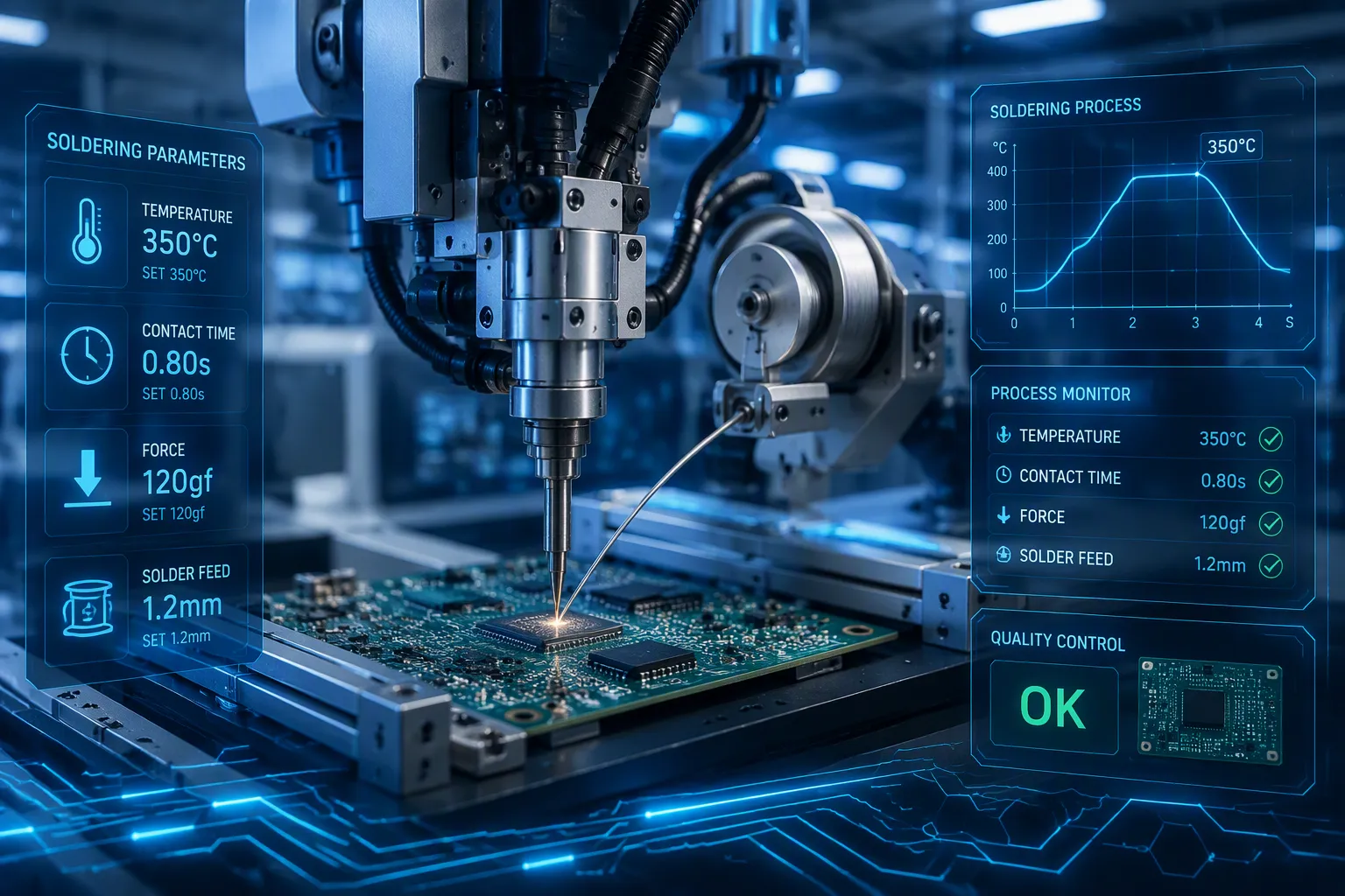
You begin robotic soldering with a tip temperature of 350°C for leaded solder. Set your contact time between one and two seconds. Apply a force of 20 to 50 grams. Synchronize solder feed with the wetting phase.
These starting points serve as your baseline, not absolute rules. You fine-tune each parameter for your specific PCB. The goal remains consistent: achieve high-quality solder joints while protecting components from thermal damage. Proper wetting requires careful balance. Too little wetting creates weak bonds. Excessive heat damages pads. You optimize robotic soldering parameters through systematic adjustment. This approach improves solder joint quality and boosts increased productivity. Remember, automated soldering demands precision. You control temperature, time, force, and feed. Each variable affects wetting quality. Master these elements for higher quality soldering. Your results improve with practice, leading to fewer defects and stronger connections.
Key Takeaways
Start with baseline settings: 350°C for leaded solder, 1-2 seconds contact, 20-50 grams force, and synchronized solder feed.
Use the lowest temperature that works to protect your PCB from heat damage.
Measure actual joint temperature with a thermocouple to verify your settings.
Adjust contact time per joint type; too short causes weak bonds, too long damages components.
Apply consistent force for reliable heat transfer and strong solder joints.
Match solder feed volume to joint size to avoid bridges or weak connections.
Optimize parameters as a system; changing one affects the others.
Tune one parameter at a time and document results for continuous improvement.
Optimize Robotic Soldering Parameters: Setting the Right Temperature
Heat control is the most critical factor you manage. The right heat level determines whether solder flows correctly and bonds with the pad. You start with a range. For most leaded solder applications, set your tip heat between 320°C and 380°C. For lead-free solder, the range is 380°C to 420°C. You follow one principle: use the lowest heat possible, but raise it when necessary. This approach minimizes thermal damage to your PCB. A higher heat melts solder faster. But it also increases risk. You can damage pads and warp the board. Lower heat protects your PCB. But it may not allow proper wetting. You find the balance through testing. Correct heat management is the foundation of solder joint quality.
Heat Transfer and Intermetallic Formation
Defining the Heat Window
The heat window is the range where soldering works well. You need enough thermal energy to melt the solder. You also need thermal energy to activate the flux. The flux cleans the metal surfaces. This cleaning allows the solder to wet the pad and the component lead. The window has a lower limit and an upper limit. Below the lower limit, solder does not melt fully. Flux does not activate. Wetting fails. Above the upper limit, you risk damage. The flux burns away too fast. Components overheat. The PCB substrate may blister. You stay within the window for each joint. Your tip heat sets the upper end. But the actual joint heat level is lower. Thermal energy travels from the tip through the joint. Some thermal energy dissipates into the board. Other thermal energy goes into the component. You must account for these losses. A good starting point gives you room to adjust. Each joint on your PCB may require a different thermal setting. You test each joint type. You measure the thermal profile. You adjust accordingly.
The Role of Solder Alloy and Flux
Your solder alloy determines the melting point. Leaded solder melts at a lower heat. Lead-free solder requires more thermal energy. You select the alloy based on your application. Your flux also matters. Each flux formula activates at a specific thermal level. Some fluxes activate at lower heat. Others need higher thermal energy. You match the flux to your soldering profile. The flux must clean the surface before the solder melts. If the flux activates too late, wetting suffers. If it activates too early, it burns away. You choose a wire with the right flux formula. This choice supports your thermal settings. The combination of alloy and flux defines your heat window. You then adjust your tip heat to deliver the right thermal energy to the joint. For robotic soldering, you can program different thermal settings for different joints. This flexibility helps you manage variations across your PCB.
Determining the Right Heat for Your PCB
Component Thermal Mass and Board Thickness
Every PCB is different. Some boards have thick copper layers. Others have thin layers. Some components have large bodies. These bodies absorb thermal energy. You must consider thermal mass. A large component needs more thermal energy. A thick board also needs more thermal energy. You raise your tip heat slightly for these joints. But you must not exceed the limit. You test each joint type. You look for proper wetting. You check for damage. You adjust heat based on results. Your PCB layout also matters. Large ground planes sink thermal energy away from the joint. This heat sinking requires a higher thermal setting or longer contact time. You treat each joint as unique. You set thermal level per joint if your system allows. This approach gives you control over your PCB assembly. Your PCB design affects every soldering decision. You account for these factors in your thermal settings.
Using a Thermocouple for Verification
You cannot guess the joint heat level. You must measure it. A thermocouple gives you real data. You attach the thermocouple wire to the joint. You run a soldering cycle. The thermocouple records the thermal profile. You see the peak heat. You see the time above liquidus. This data tells you if your settings work. You compare the measured heat to your target. You adjust your tip heat accordingly. A thermocouple verification costs time. But it saves you from defects. You use it during initial setup. You also use it when you change boards or components. This practice ensures your soldering process stays within the window. You rely on data, not guesses. Your PCB assembly benefits from this verification. You reduce rework. You increase yield. Automated soldering systems work best with verified settings.
Common Heat Mistakes and Defects
Overheating: Pad Lift and Component Damage
Overheating causes serious problems. Pad lift is one issue. The adhesive bond between the pad and the PCB fails. The pad lifts away from the board. You cannot repair this defect. The board becomes scrap. Component damage also occurs. Resistors and capacitors tolerate limited thermal energy. Exposure to high heat cracks their bodies. Internal connections break. The component fails immediately or later. You also risk intermetallic growth. A thick intermetallic layer makes the joint brittle. The joint cracks under stress. You avoid overheating by staying within your heat window. You monitor your tip heat. You verify each joint. You protect your PCB. Overheating is the most common mistake in automated soldering of PCBs. You prevent it with careful planning and verification.
Low Heat: Cold Joints and Dewetting
Low heat causes different defects. A cold joint looks dull and rough. The solder does not flow completely. It forms a poor connection. The joint may pass initial testing. But it fails under vibration or thermal cycling. Dewetting is another problem. The solder melts. It contacts the pad. But it does not bond. The solder pulls back into a ball. The pad remains exposed. This defect occurs when the heat is too low for the flux to activate. The flux cannot clean the surface. The solder cannot wet. You solve this problem by raising the thermal level. You may also need to adjust contact time. The goal is a shiny, smooth fillet. The fillet covers the pad and the lead. You achieve this result with correct heat management. You test your settings. You verify that your PCB meets quality standards. Low heat defects indicate a need to recalibrate your parameters.
Heat management is the foundation of good soldering. You set your tip heat correctly. You measure the actual joint heat level. You adjust for thermal mass. You avoid overheating and underheating. Your results improve. Your PCB assembly process becomes reliable. You produce strong joints every time. This focus on heat helps you optimize robotic soldering parameters for each application.
Contact Time: Balancing Speed and Solder Joint Quality
Contact time, or dwell time, directly shapes your solder joint quality. Too short a contact leaves you with incomplete wetting. Too long a contact damages the joint through excess heat. You start with a baseline of one to two seconds for most applications. This window gives you enough thermal energy to form a proper bond without cooking the components. Robotic systems excel here because you can program different dwell times for each joint on your PCB. This flexibility proves invaluable for high-mix, low-volume production runs where joint geometries vary widely across the board.
The Wetting Timeline: From Contact to Bond
Minimum Time for a Strong Intermetallic Bond
The wetting process follows a precise timeline. When your soldering tip touches the joint, heat begins flowing into the pad and component lead. The flux activates first, cleaning oxides from the metal surfaces. Then the solder melts and flows across the joint. Finally, the solder forms an intermetallic bond with the copper pad. This entire sequence takes time. You need enough contact for the intermetallic layer to form properly. A thin, continuous intermetallic layer creates a strong mechanical and electrical connection. If you cut the contact short, the solder may melt but never achieve proper bonding. The result is a joint that looks acceptable but fails under stress. You must allow the wetting process to complete fully.
Maximum Time Before Thermal Damage
The upper limit of contact time matters just as much. A controlled experiment on ultrasonic soldering of Sn99.7Cu0.3 samples demonstrated this clearly. Samples soldered for only 0.5 seconds exhibited more than 40% higher peel strength compared to those soldered for 10 seconds. The prolonged heat input caused overheating, oxidation, and coarsening of crystal grains in the solder alloy. These changes reduced the mechanical integrity of the joint. You face the same risk with robotic soldering. Extended contact time does not improve the bond. It degrades it. The intermetallic layer grows too thick, becoming brittle. Oxidation forms on the solder surface, creating a dull appearance. You must respect the upper boundary of your time window.
Balancing Speed and Quality in Production
Calculating Cycle Time vs. Joint Quality
Production speed creates pressure to minimize contact time. Every second you save per joint adds up across thousands of joints. But you cannot sacrifice solder joint quality for speed. A joint that fails inspection requires rework, which costs more time than you saved. You calculate your cycle time honestly. Include the contact time, the approach and retract movements, and the solder feed sequence. Compare this against your defect rate. A slightly longer contact time that reduces defects by a few percent often proves more efficient overall. You measure your yield and adjust accordingly. The optimal balance maximizes good joints per hour, not raw cycle speed.
Adjusting Time for Different Joint Geometries
Your PCB contains many joint types. A through-hole component lead requires different contact time than a surface-mount pad. A large ground plane sinks heat away quickly, demanding longer contact. A small capacitor body tolerates less heat, requiring shorter contact. You program your robotic system with per-joint dwell times. This capability lets you optimize each connection individually. You group similar joints together and assign appropriate settings. You test each group and refine the values. The result is a soldering process that respects the thermal characteristics of every component on your board.
Troubleshooting Time-Related Defects
Short Time: Insufficient Wetting and 'Blowholes'
Short contact time produces recognizable defects. Insufficient wetting leaves the solder balled up on the pad without spreading. The joint lacks the characteristic concave fillet shape. Blowholes appear when flux gases become trapped because the solder solidifies before they escape. These voids weaken the joint and create pathways for corrosion. You spot these defects during visual inspection. The fix involves increasing your contact time slightly. You also verify that your tip temperature provides enough thermal energy for the wetting process to complete within the new time window.
Long Time: Solder Wicking and Component Stress
Excessive contact time creates its own set of problems. Solder wicking occurs when molten solder climbs up the component lead, away from the joint. This leaves a starved joint at the pad surface. Component stress builds as heat conducts into the component body. Plastic packages soften and deform. Ceramic capacitors develop microcracks. These defects may not appear immediately but cause field failures later. You prevent them by keeping contact time within your verified window. You monitor your process and adjust when you see these warning signs. Your robotic soldering system gives you the precision to maintain consistent contact time across every joint.
The relationship between contact time and joint strength is clear. You find the sweet spot for each joint type on your PCB. You verify your settings with testing. You adjust based on results. This systematic approach to dwell time ensures reliable, repeatable soldering across your entire production run.
Contact Force: Ensuring Consistent Automated Soldering
Force creates the physical bridge between your soldering tip and the joint. Without proper force, heat transfer becomes unpredictable. The tip may hover above the pad, leaving an air gap that blocks thermal flow. Or the tip may press too hard, damaging the board. You need consistent mechanical pressure for consistent thermal results. This pressure ensures the tip contacts the same surface area every cycle. Your robotic soldering system applies this force automatically. You set the value in your program. The machine maintains it precisely across every joint. This consistency forms the foundation of reliable automated soldering.
The Role of Force in Thermal and Mechanical Contact
Ensuring Consistent Heat Transfer
Force directly controls thermal conductivity at the tip-to-joint interface. When you apply adequate pressure, the tip flattens slightly against the pad. This deformation increases the contact area. More surface area means more thermal energy flows into the joint. The heat transfers efficiently and evenly. Without sufficient force, the tip touches only a small portion of the pad. Heat concentrates in one spot. The rest of the joint remains cold. Solder melts unevenly. Wetting suffers. You see this problem clearly when soldering large pads or thick copper planes. These joints need more thermal energy. They also need more force to establish good thermal contact. You adjust both parameters together for best results.
Impact on Solder Joint Shape and Integrity
Force also shapes the final solder joint. When the tip presses into the molten solder, it creates a specific fillet geometry. The pressure pushes solder outward, forming a concave profile. This shape indicates proper wetting and good bond strength. Too little force leaves a rounded, convex fillet. The joint looks bulky and may hide voids. Too much force squeezes solder away from the pad entirely. You end up with a starved joint. The mechanical integrity of the connection depends on this balance. A properly formed fillet distributes stress across the entire joint area. This distribution prevents crack formation under thermal cycling or vibration. Your solder joint quality improves when you control force precisely.
Determining the Optimal Force Range
Force vs. Tip Size and Geometry
Your starting point for force is 20 to 50 grams. But this range only works for standard tip sizes. A fine tip with a small contact area needs less force. The pressure concentrates on a tiny surface. Even 20 grams may feel excessive. A large chisel tip spreads force over a bigger area. You may need the full 50 grams or more to achieve good thermal contact. You also consider tip geometry. A beveled tip contacts the joint at an angle. This shape requires different force than a flat tip. You match the force to the tip you use. You test each combination. You record the results. This data guides your future settings.
The 'Touch' Method: Using Machine Feedback
Modern robotic soldering systems offer a touch detection feature. The machine senses when the tip makes contact with the joint. It measures the force in real time. You use this feedback to find the optimal setting. Start with a low force value. Run a test cycle. Watch the machine readings. Increase the force gradually until you see consistent thermal performance. The system tells you when the tip contacts the pad reliably. You lock in that value. This method removes guesswork. You rely on data rather than intuition. The touch method works especially well for high-mix production. You can store different force values for different joints. The machine switches automatically.
Mistakes to Avoid with Contact Force
Excessive Force: Pad Damage and Solder Smearing
Applying too much force creates immediate damage. The tip can push the pad off the board entirely. This defect, called pad lift, ruins the PCB. You cannot repair it. Excessive force also smears solder across the board surface. The solder spreads beyond the pad area. This creates bridges between adjacent traces. Short circuits follow. You also risk damaging the component itself. A heavy tip can crack a ceramic capacitor or bend a delicate lead. You avoid these problems by staying within your verified force range. You monitor the machine feedback. You adjust when you see signs of stress.
Insufficient Force: Inconsistent Heating and Cold Joints
Too little force produces subtler defects. The tip makes poor contact with the pad. Heat transfers inconsistently. Some areas of the joint reach temperature. Others stay cold. The solder melts partially. It forms a grainy, dull surface. This cold joint looks weak and performs poorly. It may pass visual inspection but fail under load. You also see inconsistent results across multiple joints. The same program produces different outcomes. This variability indicates a force problem. You increase the force slightly. You verify the improvement. Your soldering process becomes repeatable. Every joint receives the same thermal treatment.
Force management transforms your robotic soldering results. You set the correct pressure for each tip and joint combination. You verify with machine feedback. You avoid the extremes of too much and too little. Your solder joints become stronger and more consistent. This attention to force completes your parameter optimization.
Solder Feed: Controlling Volume for Your PCB
Solder feed controls material volume at each joint. Feed rate and timing determine this volume. Too much material causes bridges. Too little leaves joints weak. You match the feed to each joint on your PCB. Wire diameter matters. A larger wire delivers more material per unit length. Flux percentage affects wetting behavior. You select the right wire for your joint sizes. This selection supports your soldering process. This attention to feed timing improves your solder joint quality.
Feed Rate, Timing, and Joint Size
Synchronizing Feed with the Wetting Phase
Timing matters in solder feed. You deliver the wire when the joint reaches temperature. Flux activates first. Flux cleans the metal surfaces. This cleaning allows proper wetting to occur. You feed the wire after flux activates but before heat dissipates. This synchronization ensures material flows into the gap. Capillary action pulls material through the joint. Complete wetting fills the connection area. You program the feed start point carefully. A half-second delay changes the result. The joint may suffer from poor wetting. You test each joint type. You record the ideal feed timing. Your robotic soldering system applies this timing consistently.
Calculating Volume for Different Joint Types
Each joint type needs a specific volume. A through-hole joint requires more material. The hole fills with the alloy. The fillet forms on both sides. You calculate the volume from hole diameter, board thickness, and pad size on your PCB. A surface-mount joint needs less material. You estimate volume from pad dimensions and component width. You select the wire diameter that delivers this volume. A 0.5mm wire delivers a controlled amount per millimeter. A 0.8mm wire delivers more. You match the wire to the joint. You adjust feed length until the joint looks correct. The component lead shows a visible wetting line.
Programming the Feeder for Precision
Adjusting Feed Speed and Retraction Distance
The feeder gives you two controls. Feed speed determines how fast the wire moves toward the joint. Retraction distance determines how far the wire pulls back. You set speed based on joint size. A large joint accepts faster feed. A small joint needs slower feed. Retraction distance prevents material from dripping. You set this distance to clear the molten pool. The wire retracts. The material breaks cleanly. You test these settings during automated soldering. Good programming produces the same result every time. Your PCB assembly benefits from this precision.
Using Pre-forms vs. Wire Feed
Wire feed works for most applications. Some joints benefit from pre-forms. A pre-form is a solid piece of alloy shaped for a specific joint. You place it on the pad before soldering. Heat melts the pre-form. The alloy flows into the joint. Pre-forms work well for through-hole connectors. Wire feed offers more flexibility. You change volume by adjusting feed length. You choose the method that fits your production. High-mix boards benefit from wire feed. High-volume runs benefit from pre-forms.
Common Feed Defects and Solutions
Overfeeding: Bridges and Balls
Feeding too much material creates problems. Excess material spreads beyond the pad. It touches adjacent pads or traces. This creates a bridge. The bridge causes a short circuit. Small spheres also break away from the main joint. They roll across the board surface. They lodge under components. You prevent overfeeding by reducing feed length. You also check your wire diameter. A smaller wire gives finer control. The correct amount fills the joint without overflow.
Underfeeding: Starved Joints and Insufficient Fillet
Feeding too little material leaves a starved joint. Material does not cover the pad completely. The fillet appears concave but thin. The component lead may show a gap. This joint lacks strength. It cracks under stress. The connection may fail over time. You solve underfeeding by increasing feed length. You add small increments. You inspect each test joint. The material should wet the entire pad surface. Proper wetting indicates sufficient volume. You stop when the joint looks correct. Your PCB receives reliable connections.
Feed control gives you precise volume management for your PCB. You synchronize with the wetting phase. You calculate the right amount for each joint. You program your feeder for consistent results. The result is a better soldering process.
The Interplay of Parameters: A Systems Approach
Temperature, time, force, and feed do not work in isolation. Each parameter shifts the others. A higher temperature setting demands a shorter contact time to prevent damage. A larger tip requires more force to maintain thermal contact. You must view these variables as one interconnected system, not four separate controls.
How Temperature, Time, Force, and Feed Affect Each Other
The Thermal Balance: Time and Temperature as a Pair
Temperature and time form a paired relationship. You can achieve the same thermal energy delivery with high heat over a short duration or lower heat over a longer duration. The difference lies in the risk profile. High heat with short contact reduces cycle time but narrows your margin for error. Low heat with extended contact protects sensitive components but slows production. Consider wave soldering as an example. A solder pot temperature of 250–260°C paired with a dwell time of 3–5 seconds produces reliable joints. Preheat on the topside reaches 120–150°C. The conveyor angle sits at 6–8 degrees. These settings work together. Change one value, and the others must shift to compensate. Your pcb assembly demands this balance.
The Mechanical Balance: Force and Feed for Consistency
Force and feed operate as a mechanical pair. Proper force ensures the tip maintains stable contact with the joint. This stability creates a consistent thermal path. Your solder feed then delivers material into a predictable molten pool. If force fluctuates, the gap between tip and pad changes. Heat transfer becomes erratic. The solder may not wet properly. You compensate by adjusting feed timing, but this approach only masks the root cause. Instead, you stabilize force first. Then you fine-tune process parameters for feed. This sequence produces repeatable results across every joint on your pcb.
The Role of Approach Angle and Fixture Repeatability
Optimizing Tip Approach for Consistent Contact
The angle at which your tip approaches the joint affects every other parameter. A perpendicular approach delivers force evenly across the pad surface. An angled approach concentrates pressure on one edge. This uneven pressure distorts heat flow. You must program a consistent approach angle for each joint type. Your robotic soldering system repeats this angle precisely. The result is uniform thermal and mechanical contact. Your solder joint quality improves because every cycle behaves identically.
Ensuring Repeatable Fixture Location for High-Mix Production
Your fixture determines whether the pcb sits in the same position every cycle. A loose fixture allows board movement during soldering. The tip contacts a slightly different location each time. This variability ruins your parameter settings. You tighten fixture tolerances. You verify board position before each cycle. High-mix production demands this rigor. Different boards require different fixtures. Each fixture must locate the pcb with the same precision. This consistency enables your programmed parameters to work as intended.
A Practical Workflow for Process Optimization
Step-by-Step Tuning: From Baseline to Final Settings
Start with your baseline values. Set temperature at 350°C for leaded solder. Use a contact time of 1–2 seconds. Apply 20–50 grams of force. Synchronize feed with wetting. Run test joints. Inspect each one. Adjust one parameter at a time. Change temperature first. Observe the effect. Then adjust time. Then force. Then feed. Document every change. This methodical approach prevents confusion about which variable caused which result. A reported pilot program across multiple electronics manufacturing facilities measured a first-pass yield improvement of +5.2 percentage points after 90 days of systematic optimization. The yield rose from 91.3% to 96.5% at post-reflow inspection. You can achieve similar gains with disciplined tuning.
Using Data and Process Monitoring for Continuous Improvement
Your optimization work never truly ends. You collect data from every production run. You track defect rates. You monitor thermal profiles. This information guides your next adjustment. Automated soldering systems generate this data automatically. You review it regularly. You spot trends before they become problems. This continuous improvement cycle drives increased productivity. Your pcb assembly process becomes more efficient with each iteration. You achieve higher yields and fewer defects. The systematic approach transforms soldering from guesswork into engineering.
You now understand the four pillars of robotic soldering. Temperature, contact time, force, and solder feed work together as one system. No single magic number exists. Each application has its own sweet spot. You find it through measurement, adjustment, and verification.
Start with your baseline settings. Test each joint. Change one parameter at a time. Document every result. This iterative approach helps you optimize robotic soldering parameters for your specific pcb. You achieve high-quality solder joints while protecting components from thermal damage. Improving solder joint quality becomes your daily focus.
Mastering these elements unlocks the full potential of automated soldering. You reduce defects, increase yields, and boost increased productivity. Apply this systematic method to your own pcb assembly. Your soldering improves with each cycle. Higher quality soldering becomes your standard. Start optimizing today.
FAQ
What is the best starting temperature for robotic soldering?
Start with 350°C for leaded solder. Use 380-420°C for lead-free alloys. These values give you a baseline. You adjust from there based on your specific PCB and components. Measure the actual joint temperature with a thermocouple to verify your settings.
How do I know if my contact time is too short?
Inspect the joint surface. A dull, grainy appearance signals incomplete wetting. You might see solder balled up without spreading. Blowholes indicate trapped flux gases. Increase your dwell time by 0.2-0.3 seconds and test again. The fillet should look smooth and concave.
What happens if I apply too much force during soldering?
Excessive force can lift pads from the board. This defect ruins the PCB permanently. You might also smear solder across adjacent traces, creating short circuits. Watch your machine feedback readings. Reduce force if you see pad stress or component damage during automated soldering.
Why does my solder feed timing matter so much?
Feed timing determines whether solder flows into the joint properly. You must deliver wire after flux activates but before heat dissipates. This synchronization allows capillary action to pull material through the connection. A half-second delay changes the entire wetting result. Test each joint type to find the ideal timing.
Can I use the same parameters for every joint on my PCB?
No. Different joints need different settings. A through-hole component lead requires more heat and material than a surface-mount pad. Large ground planes sink heat away quickly. Your robotic system lets you program per-joint values. Group similar joints together and assign appropriate parameters for each group.
How often should I recalibrate my soldering process?
Recalibrate whenever you change boards, components, or solder wire. Also verify settings after any maintenance on your soldering equipment. Monitor defect rates continuously. A rise in cold joints or bridges signals drift in your process. Regular data review helps you optimize robotic soldering parameters before problems escalate.
What is the fastest way to improve my soldering yield?
Change one parameter at a time. Document every adjustment you make. Run test joints after each change. This methodical approach reveals which variable affects your results most. Track your first-pass yield data. Systematic tuning consistently improves quality across production runs.
See Also
Essential Temperature Curve Specifications for SMT Reflow Soldering
Key Process Demands for Reflow Soldering in SMT Manufacturing
The Influence of Precise Temperature Profiling on SMT Reflow Quality
Procedures for Testing Real-Time Reflow Temperature Curves in PCBA Production
Expert Technical Guidance for Wave Soldering in SMT Assembly
