High-Speed Signal Design Guidelines for Server PCBs
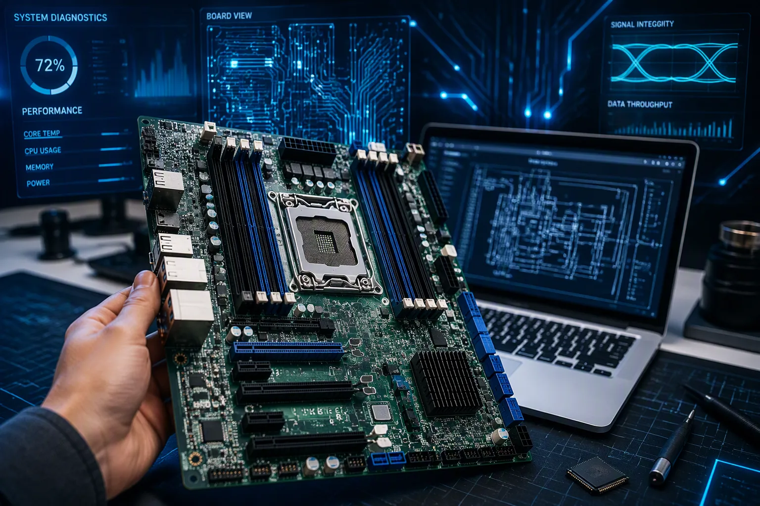
Designing faster, denser server boards for data centers and AI workloads is a huge challenge. Will your high-speed 25Gbps SerDes link work on the first try? At these high speeds, wires act like transmission lines, and signal integrity issues such as reflection, ringing, crosstalk, and insertion loss take over the signal. This guide offers practical high-speed PCB design tips for mastering stackup, routing, and common mistakes. Focus on high-speed PCB layout, high-speed PCB stackup, and routing. You will get better at high-speed signal quality in high-speed designs for high-speed uses. By the end, you will have a checklist to use on your next server board, helping you succeed on the first attempt. This high-speed performance is essential.
Key Takeaways
The rise time, not the clock speed, is what decides if a signal is high-speed.
Use low-loss materials and solid ground planes in your stackup.
Route differential pairs with steady spacing and equal lengths.
Back-drill vias to take off extra metal pieces, called stubs, and make the signal work better.
Never route over plane splits; use stitching capacitors if needed.
Defining High-Speed Signals and Signal Integrity
Rise Time vs. Clock Frequency
Many engineers think clock frequency decides when a signal becomes high-speed. That idea is not correct. The real factor is rise time. A trace with a fast edge can act like a high-speed signal even at a low clock speed. Rise time alone tells high-speed signals apart from low-speed ones. Clock frequency does not directly affect signal integrity.
The 3 dB bandwidth goes down as rise time goes up, and you can find it with 3 dB bandwidth = 0.35/tr. For instance, a 1 ns rise time gives a 350 MHz bandwidth. That means the trace can send frequencies up to 350 MHz without losing much strength.
This link shows why faster rise times lead to higher bandwidths. A short rise time lets higher-frequency parts travel. That behavior creates signal integrity problems in your high-speed designs.
Rise time is the only thing that separates high-speed from low-speed signals.
Faster rise times cause stronger crosstalk in nearby channels. This effect does not depend on data rate or clock rate.
In high-speed pcb design, you must treat every trace with a fast edge as a transmission line. Ignoring rise time leads to bad signal quality and failed links.
Transmission Line Effects and Critical Length
When trace length goes past a certain point, reflections and ringing happen. That point is the critical length. You can figure it out with several rules.
Rule | Formula/Expression | Condition/Application |
|---|---|---|
1/10 rule | Critical length = λ/10 | Safe to ignore impedance mismatch for traces shorter than this |
Digital edge rule | Critical length = function of rise/fall time | Used when working with digital traces |
1/16 rule | Critical length = λ/16 | Good estimate for PCB traces with impedance under 110 Ohms |
Past the critical length, your trace becomes a transmission line. Impedance changes along the path make part of the signal bounce back toward the source. This causes ringing and distortion. The problem gets worse as rise time gets shorter.
Ringing and distortion can break logic thresholds or timing needs. This causes logic errors in high-speed server PCB traces.
To fix these issues, keep controlled impedance steady. Keep the return path continuous and near the signal layer. Match source and receiver impedances. Use proper termination methods. Reduce problems from vias and stubs. Use differential signaling with tightly coupled pairs.
For any high-speed pcb, impedance matching is very important. You must plan your routing for every trace. Every discontinuity hurts signal quality. Your stackup design and trace routing decide if your high-speed digital designs work or fail. A good high-speed pcb stackup supports clean signal transmission.
High-Speed PCB Stackup Design for Controlled Impedance
The stackup you pick for your high-speed pcb design decides if your signals arrive clean or get distorted. Every high-speed connection needs a steady environment. You must think about material choice and layer setup from the start. Controlled impedance routing depends on the stackup structure. Without careful planning, your high-speed pcb will fail.
Material Selection for Low-Loss Performance
Standard FR-4 becomes a problem for data rates above 10 Gbps. The dielectric loss is too high. You need low-loss materials for reliable transmission. For 28 Gbps NRZ signaling, Panasonic Megtron 6 works well. Its dissipation factor is 0.004 at 12 GHz. This keeps your signal clean for trace lengths over 3 inches. Megtron 6 belongs to the low-loss material class. Its dissipation factor is very low. This makes it suitable for long traces. A hybrid stackup can save cost. Use low-loss material only on signal-layer dielectrics. Use standard FR-4 on power-plane dielectrics. This reduces material cost by 20-30% without compromising performance. A high-speed pcb requires careful material selection.
For 10-28 Gbps NRZ, you need materials with Df below 0.010 at 14 GHz. Mid-loss materials like Megtron 4, EM-370D, or S1170G work for shorter traces. For longer traces above 3 inches, upgrade to low-loss materials like Megtron 6. For 56 Gbps PAM4 links, the material choice becomes even more critical. Low Dk material enables wider traces on thinner layers. This reduces skin effect and extends bandwidth. Copper roughness becomes the dominant loss mechanism on low-loss laminates. Smooth HVLP copper improves impedance matching at high frequencies. Good impedance matching reduces reflections. Good impedance matching also improves power transfer. Material parameter variations in Dk and roughness factor are significant contributors to loss and variations. These variations affect your design directly.
Layer Arrangement and Plane Adjacency
Every signal layer must sit next to a solid plane layer. This plane provides a continuous return path. It minimizes EMI. A solid ground plane maintains the proper environment. It keeps the trace clean. For a 6-layer stackup, alternating layers reduces crosstalk by up to 25%. Return currents flow directly under the trace. This prevents unpredictable paths and distortion.
Uniform conditions are required to ensure traces travel cleanly, without reflections, distortion, or timing errors. If conditions vary from one point to the next, a reflection occurs whose magnitude depends on the difference.
Without a solid ground plane, return currents find unpredictable paths. This creates large current loops. These loops radiate EMI. Fractured return paths enlarge current loops. This increases radiation. The larger the loop, the more EMI. Proper via stitching reduces these loops. Common disruptions include split ground planes, improper layer hopping without return vias, and traces around board cutouts. These cause excessive EMI, ringing, crosstalk, and ground bounce. Multiple prototypes with fully controlled routing still failed EMC certification due to fractured return paths. The high-speed pcb design must include via stitching. Use via stitching along ground plane edges. The pitch should be between lambda/20 and lambda/10. This provides multiple low-return paths. Ensure ground pours connect properly to the main ground network. This prevents isolated regions from acting as unintended antennas.
High-Speed PCB Design Routing Best Practices
Now you move from stackup planning to the actual trace layout. This stage decides whether your high-speed signal arrives clean or degrades into noise. You need strict rules for differential pairs and careful management of vias. These high-speed routing guidelines separate working boards from failed prototypes.
Differential Pair Routing and Length Matching
Differential pair routing demands constant spacing between the two traces. You must keep the gap uniform along the entire path. Any change in spacing alters the differential impedance. That change causes reflections. For 100-ohm differential pairs, you should target a spacing that produces the correct impedance for your stackup. You also need to match the lengths of both traces in the pair. Length mismatch creates skew. Skew converts differential signals into common-mode noise. This noise radiates and degrades your signal.
You should route both traces of a pair on the same layer. Do not split them across layers. Different layers mean different dielectric environments. That difference creates timing skew. You also need to avoid routing over plane splits. A split plane breaks the return path. The current must find another route. That detour creates a loop antenna. The loop radiates noise and increases EMI.
Critical warning: Routing differential pairs over split ground planes disrupts the low-impedance return path, creating a 'loop antenna' effect that significantly increases noise. Mitigation: If a split cannot be avoided, route traces carefully around the split or use stitching capacitors to bridge the gap, ensuring the capacitor is positioned to keep the forward and return path separation minimal.
For mixed-signal boards, you should keep analog and digital grounds separate. Connect them at a single point. Use a zero-ohm resistor or a ferrite bead. Never route digital signals over analog ground planes. This violation breaks return path integrity. Your high-speed pcb design must respect these boundaries.
Crosstalk Reduction and Via Management
Crosstalk reduction starts with spacing. You need enough distance between aggressor and victim traces. A common rule is 3W spacing. This means three times the trace width between centers. This spacing provides significant protection. It works best when a ground plane exists on the next layer. Guard traces can help, but only in specific cases. A guard trace works in stripline when both ends connect to ground. This helps with near-end crosstalk. For far-end crosstalk, the reduction is small. The crosstalk is already low in that configuration. So you should rely on spacing first. Guard traces are a secondary tool.
Via management is equally important. A via stub acts like a transmission line stub. It reflects energy back to the signal. At 25 Gbps, a 0.5 mm stub creates a resonance at about 11 GHz. This frequency sits inside your operating band. The resonance causes severe insertion loss and jitter. You must remove these stubs. Back-drilling is the solution. This process drills out the unused portion of the via barrel. You should target a residual stub of 10 mil or less. This pushes the resonance above 50 GHz. That frequency stays outside your 25 Gbps band.
Metric | With ~0.5 mm Stub | Backdrilled (<0.15 mm) | Improvement |
|---|---|---|---|
Resonance Frequency | ~11 GHz (in-band for 25 Gbps) | Eliminated in band | None |
Insertion Loss @ 5 GHz | –3.5 dB | –1.8 dB | 1.7 dB better |
Peak-to-Peak Jitter | 18 ps | 9 ps | 50% reduction |
Eye Height | 0.55 UI | 0.78 UI | +42% |
The theoretical rule says stubs should be 1/10 of the signal wavelength. For 25 Gbps, the wavelength is about 24 mm in FR4. So anything longer than 2-3 mm needs removal. Production tolerances for back-drilling range from 4-8 mil. This is the practical limit for depth accuracy. You should specify back-drilling for every high-speed via in your design. This step alone can save your link.
These routing best practices form the core of your high-speed pcb layout. Apply them consistently. Your high-speed designs will perform reliably. Your signal will arrive intact. Your impedance matching will hold across the entire path. This attention to detail makes the difference between a working server and a costly re-spin.
High-Speed PCB Design Guidelines: Avoiding Common Mistakes
Even skilled engineers make errors that ruin high-speed signal quality. Two mistakes cause most failures: routing over plane splits and ignoring loss parameters. You must understand both to succeed on the first try. These high-speed pcb design guidelines will help you avoid costly re-spins.
Routing Over Plane Splits and Its Consequences
Splits or holes in ground planes create uneven areas that raise impedance. These breaks force the return current to take detours. The detours enlarge loop areas and greatly increase inductance. High-speed traces then act like antennas that radiate electromagnetic waves. This failure mode often shows up only during EMC testing.
Never route signals across a reference plane split — if unavoidable, place a stitching capacitor at the crossing point. Return current does not care about your stackup intentions — it follows physics. If you do not provide a path, it will find one — and that path will radiate.
You must check your high-speed pcb layout for every plane gap. Look for vias that create holes in reference planes. Examine areas near board cutouts and mounting holes. Each discontinuity threatens your signal integrity. A 10-layer server board with a split power plane can fail certification despite perfect routing elsewhere. The fix requires adding stitching vias along the split edge. This restores the low-impedance return path and reduces EMI.
Ignoring Insertion Loss and Return Loss
Insertion loss comes from dielectric and conductor losses. Return loss comes from impedance mismatches. Both become critical at high speeds. Ignoring them leads to link failures. You must treat these parameters as first-class design constraints.
Return Loss (dB) | Reflected Power (%) | Effect on Signal |
|---|---|---|
20 dB | 1% | Minimal impact on eye opening |
10 dB | 10% | Noticeable reflections, reduced eye opening |
6 dB | 25% | Significant reflections, severe ISI and jitter |
Reflections create delayed signal copies that interfere with the direct signal. This reduces eye opening, causes inter-symbol interference, and adds deterministic jitter. Multiple reflections between discontinuities can cause resonant dips in insertion loss. These dips destroy the eye pattern.
Simulation tools help you catch these problems before fabrication. In a 10-layer PCB for a server application, post-layout simulation using HyperLynx revealed a trace near a power plane exhibiting 53 ohms impedance instead of the target 50 ohms. This prompted a localized redesign of trace spacing. For PCIe Gen 4 designs at 16 GT/s, TDR simulation in ANSYS SIwave detects sudden impedance changes at via transitions. You can then add stitching vias or adjust the layout for smoother signal flow.
Your high-speed routing must maintain consistent impedance matching throughout the entire path. Check every connector, via, and transition point. These guidelines apply to every high-speed pcb you design. Following routing best practices prevents signal integrity challenges before they start. Reducing crosstalk and managing differential pairs properly will protect your signal quality. Your design will work reliably when you respect these rules.
Rise time defines high-speed signal behavior, not clock frequency alone. Your stackup needs low-loss materials and solid plane adjacency. Your routing demands strict differential pair rules and careful via management.
These guidelines separate working servers from costly prototypes. Apply them as a checklist on your current project. Maintain consistent trace width. Route differential pairs with uniform spacing. Minimize vias and add ground return vias. Never route over plane splits. Match pair lengths to avoid skew.
Use simulation tools before fabrication. They reveal impedance mismatches and signal integrity challenges early. Your high-speed pcb design delivers clean signal quality. Mastering these fundamentals ensures your high-speed pcb performs reliably. Your next high-speed pcb will succeed on the first spin. This design approach prevents signal loss and reflection. Good design habits make the difference.
FAQ
How do I know if my trace is a transmission line?
You can calculate the critical length using the rise time of your signal. If your trace exceeds this length, you must treat it as a transmission line. Use the 1/10 rule as a starting point. This rule states that critical length equals one-tenth of the signal wavelength.
What stackup materials work best for 25 Gbps links?
You need low-loss materials with a dissipation factor below 0.010 at 14 GHz. Megtron 6 works well for long traces. For shorter traces, mid-loss materials like Megtron 4 or EM-370D perform adequately. A hybrid stackup saves cost by using low-loss material only on signal layers.
Why does my differential pair need constant spacing?
Constant spacing maintains the differential impedance at your target value. Any change in the gap alters impedance and causes reflections. You also need matched lengths to prevent skew. Skew converts your differential signal into common-mode noise, which radiates and degrades your signal quality.
When should I specify back-drilling for vias?
You should specify back-drilling for every high-speed via in your design. A 0.5 mm stub creates a resonance near 11 GHz, which sits inside your 25 Gbps operating band. Back-drilling reduces the residual stub to 10 mil or less. This pushes the resonance above 50 GHz.
How does routing over a plane split affect my signal?
A plane split forces return current to take a detour. This detour enlarges the current loop and increases inductance. Your trace then acts like an antenna that radiates EMI. You should never route high-speed signals across a split. If you must cross, place a stitching capacitor at the crossing point.
See Also
Proven Practices for Optimizing SMT Assembly Lines in PCBA
Critical Requirements for PCBA Processing in Medical Devices
Key Steps for Assembling Flexible PCBs to Achieve Maximum Performance
Important Technical Considerations for HDI PCB SMT Assembly
Designing PCB Boards for Manufacturability to Meet SMT Processing Needs
