Common Causes of Wire-to-PCB Solder Joint Failure
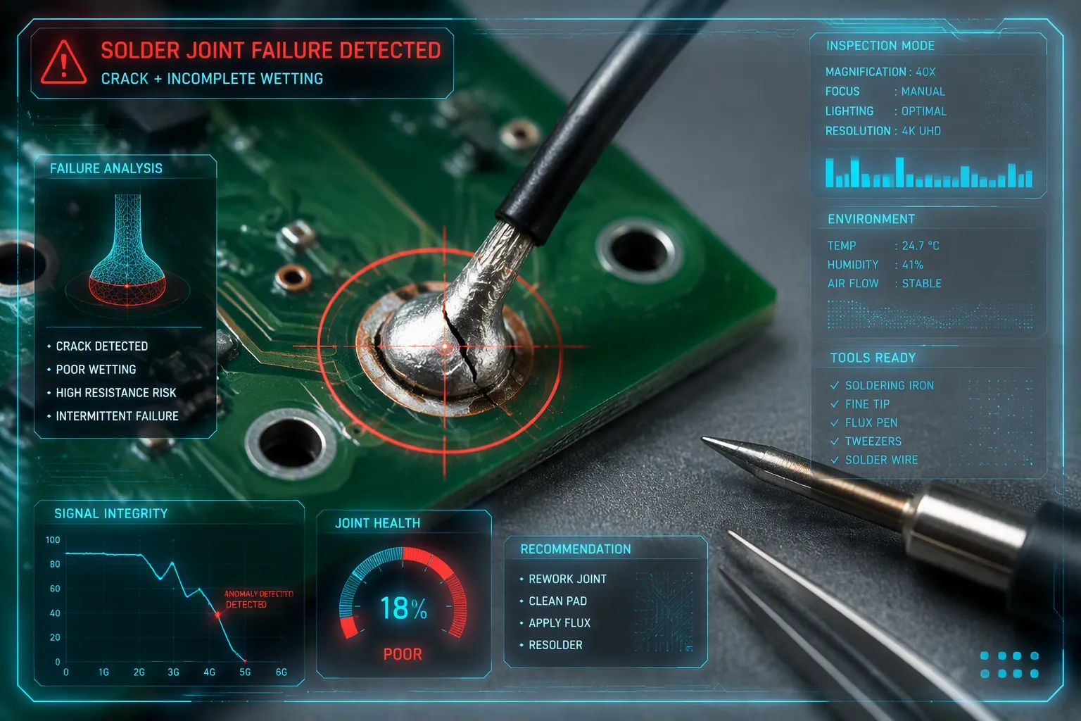
Wire-to-PCB solder joint failure can cause intermittent connections or complete loss of function in your electronics. You need to identify the root causes to maintain product quality. Thermo-mechanical fatigue is the most frequent reason for these failures, but other issues like defects, environmental exposure, and material problems also play a part. Understanding the mechanisms behind each issue helps you implement preventive measures. Designing for thermal cycling and using proper strain relief can mitigate stress. Your attention to quality during assembly reduces rework costs and extends the life of your assemblies. Root cause analysis is essential for solving recurring problems. You can detect early signs through visual inspection or electrical testing. Taking corrective action early prevents costly field failures. This proactive approach ensures reliable connections.
Key Takeaways
Thermo-mechanical fatigue causes most wire-to-PCB solder joint failures from daily temperature swings.
Dry solder joints result from low heat, poor flux, or dirty surfaces; you can prevent them with proper technique.
Design with matched expansion rates and strain relief to reduce stress from thermal cycling.
Vibration and shock create overstress cracks; use clamps or damping materials to protect joints.
Humidity and corrosion degrade joints; apply conformal coatings to block moisture.
Solder alloy and PCB finish directly affect joint strength; choose ENIG for high-reliability needs.
Pad size and wire gauge must match thermal mass to avoid weak bonds and early failure.
Post-soldering inspection with X-ray and pull testing catches hidden defects before they cause field failures.
Mechanical Stress and Wire-to-PCB Solder Joint Failure
Thermo-mechanical fatigue is the most frequent cause of wire-to-pcb solder joint failure. You encounter this problem in automotive and aerospace applications. An engine control module under the hood experiences temperature swings from subzero cold to intense heat every day. Each cycle stresses the joint.
Thermo-Mechanical Fatigue
Thermal Expansion Mismatch
The pcb, wire, and filler metal expand at different rates when heated. The board has a higher coefficient of thermal expansion than the alloy. This mismatch creates shear strain at the joint interface. You cannot eliminate the mismatch, but you can manage it through careful design choices.
Fatigue Crack Propagation
Repeated thermal cycles cause cracks to grow slowly. The crack starts at a stress concentration point, often at the heel of the fillet. Each cycle extends the crack further. The modified Engelmaier fatigue model predicts solder joint fatigue life under thermal cycling using only two parameters: total shear strain and the modified fatigue ductility exponent. This model works well for lead-free connections and gives conservative results. You can use it to estimate the lifetime of your connections before failure occurs.
Design for Thermal Cycling
You design for thermal cycling by selecting materials with matched expansion rates. Use a board with a lower CTE. Choose a ductile alloy. Add strain relief features to the wire. You can also use a larger fillet size to distribute stress. These steps improve solder joint reliability.
Vibration and Mechanical Overstress
Resonance and Shock Damage
Vibration creates mechanical stress that damages joints. When vibration frequency matches the natural frequency of the assembly, resonance occurs. The amplitude increases dramatically. Shock events like dropping the product also cause sudden stress. Both can crack the joint instantly.
PCB vibration testing, governed by standards such as MIL-STD-202, is used to assess the durability and reliability of components. The mechanical stress induced by vibrations can lead to the degradation or failure of individual components, such as solder joints. Vibration testing helps identify weak points that might fail under real-world conditions, revealing problems with solder joint integrity and connection integrity.
Identifying Overstress Cracks
Overstress cracks look different from fatigue cracks. They appear as clean, sharp fractures. You can spot them with visual inspection under magnification. The crack often runs through the bulk material rather than along the intermetallic layer.
Strain Relief and Damping
You prevent vibration damage by adding strain relief. Secure the wire to the board with a clamp or adhesive. Add damping materials to absorb vibration energy. Use conformal coatings for mechanical support. These measures extend the reliability of your connections.
Stresses from Potting and Coatings
Coefficient of Thermal Expansion Mismatch
Potting compounds, underfills, and conformal coatings protect your assembly. But they can introduce unintended stresses. The potting material has its own CTE. If it differs from the board or the joint, it creates stress during temperature changes. The stress can be significant enough to pull the solder joint apart.
Curing Shrinkage Effects
Potting compounds shrink as they cure. This shrinkage pulls on the joint. The stress can cause immediate cracking or weaken the joint for future cycles. You can reduce this effect by using low-shrinkage formulations. Always check the manufacturer data sheet for shrinkage values.
Material Selection for Reducing Stress
Choose potting materials with a CTE close to the board and the filler metal. Use flexible coatings for delicate assemblies. Test the combination before full production. This attention to quality prevents hidden stress that reduces product lifetime. Consistent quality in material selection gives you a more reliable assembly.
Solder Joint Defects and Failure
You can prevent many failures by understanding the common causes of dry solder joints. A dry solder joint occurs when the alloy fails to bond properly. You can identify dry solder joints by their grainy or dull appearance. The common causes of dry solder joints include insufficient heat, poor flux activation, and surface contamination. Learning these common causes of dry solder joints helps you improve your process.
Common Causes of Dry Solder Joints
Insufficient Heat and Flux Activation
When you do not apply enough heat, the alloy does not melt completely. The flux fails to activate and remove oxides. The result is a dry solder joint. You need to preheat the iron to at least 15°C above the alloy melting point. This ensures proper wetting. A dry solder joint from insufficient heat looks dull and grainy.
Surface Contamination Effects
Grease, dust, or oxidation on the surfaces prevents the filler metal from bonding. Contamination leads to a dry solder joint. You can avoid this by cleaning the wire and pad with a solvent before soldering. Store materials in a dust-free environment. A contaminated surface produces a dry solder joint that lacks strength.
Proper Soldering Technique
Apply the correct amount of filler metal and heat. Move the iron smoothly. Do not move the joint during cooling. A dry solder joint often results from poor technique. You can identify dry solder joints by their appearance and test them for continuity. Use proper technique to achieve a reliable connection.
Insufficient Wetting and Poor Adhesion
Solder Resist and Oxide Layers
Solder resist stains and metal oxide layers prevent proper wetting. Oxide layers form on the wire and pad over time. You must remove them with flux. Contaminated flux or paste also causes poor adhesion. The result is a dry solder joint with weak mechanical strength. You can inspect the joint for signs of non-wetting. The filler metal does not spread evenly. One of the common causes of dry solder joints is poor wetting. This is a primary cause of wire-to-pcb solder joint failure.
Signs of Incomplete Wetting
You can identify incomplete wetting by the shape of the fillet. The filler metal does not climb the wire or cover the pad. The joint looks like a ball sitting on the surface. This is a dry solder joint. You can also check for electrical resistance. High resistance indicates poor wetting. This compromises solder joint reliability.
Surface Preparation for Adhesion
Clean the surfaces before soldering. Use a solvent to remove grease. Abrade the wire to remove oxide. Apply flux to the joint area. Proper preparation leads to a strong bond. A dry solder joint from poor adhesion can be prevented. This is one of the preventive measures of dry solder joints.
Voids and Porosity
Outgassing and Flux Entrapment
Voids form when gas becomes trapped in the filler metal. Outgassing from the board or flux entrapment creates these pockets. The chart below shows how different test methods affect void-related failures.
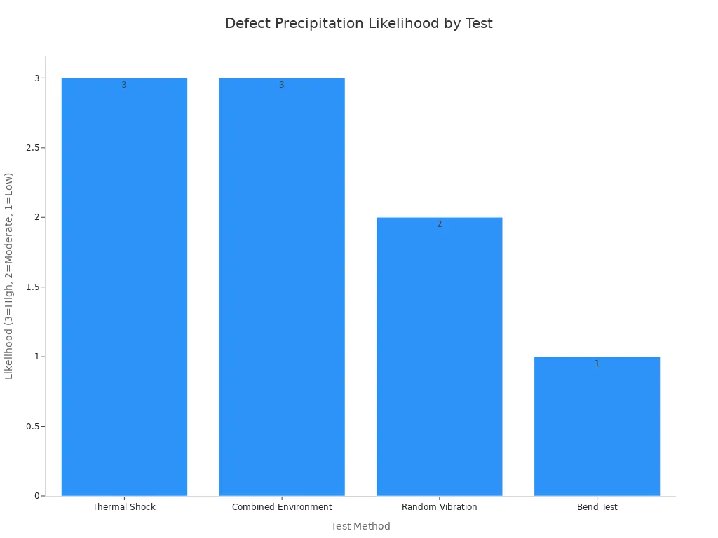
Voids reduce the effective cross-sectional area. This weakens the joint. A dry solder joint with voids is more likely to fail.
Impact on Mechanical Strength
Voids concentrate stress. Under thermal cycling, cracks start at the void edge. The joint fails earlier. This reduces solder joint quality. You can use inspection methods like X-ray to detect voids. Visual inspection alone is not enough. A clean pcb surface reduces void formation. Inspect the pcb for defects before soldering.
Void Reduction Strategies
You can reduce voids by controlling the reflow profile. Preheat the board to drive out moisture. Use a vacuum during soldering. Clean the surfaces to remove contaminants. These are important preventive measures of dry solder joints. Voids increase the risk of failure. Implement quality control procedures. Improve overall assembly quality. Voids also reduce long-term reliability.
Environmental Factors in Solder Joint Failure
Temperature extremes and humidity create harsh conditions for your connections. Environmental exposure accelerates degradation and reduces the lifetime of your assemblies. Understanding these factors helps you design for real-world conditions.
Temperature Extremes and Cycling
Coefficient of Thermal Expansion Mismatch
The pcb, wire, and solder alloy each expand at different rates when temperatures change. This mismatch creates mechanical strain at the joint interface. During unexpected temperature cycling, the repeated expansion and contraction stresses the connection. You cannot eliminate this mismatch entirely. You can manage it through material selection and joint geometry.
Failure Under Repeated Cycles
Typical lead-free solder joints can withstand 1,000 to 3,000 thermal cycles between -40°C and 125°C before failure, depending on material and design parameters. During high-low temperature cycling, the solder undergoes microstructural coarsening at high temperatures, forming a coarse crystal zone. Cracks originate at the Sn-rich phase or grain boundaries after repeated cycles. The high-temperature stage promotes isomerization and coarsening, leading to crack initiation. Notably, the thickness of the interfacial metal compound layer has negligible effect on thermal fatigue. The residence time at high temperature does not significantly influence fatigue life either. This supports the use of accelerated thermal cycle tests to study solder fatigue behavior.
Under low-cycle isothermal mechanical fatigue, the fatigue life of eutectic tin-lead solder decreases linearly as temperature increases. Increasing frequency from 10⁻⁴ Hz to 10⁻³ Hz also linearly reduces fatigue life. Further increasing frequency from 10⁻³ Hz to 1 Hz produces only a small improvement in fatigue life.
Thermal Management Solutions
You can extend solder joint reliability by managing temperature excursions. Use thermal management techniques to reduce the temperature range the joint experiences. Heat sinks, thermal vias, and proper airflow all help. For qualification testing, follow established standards:
Standard | Role in Thermal Cycling Testing |
|---|---|
IPC-9701 | Qualification and performance test methods for surface mount solder attachments |
JEDEC JESD22-A104 | Standardized temperature cycling conditions for testing |
Following these protocols ensures standardized, repeatable results for qualification. Engineers predict reliability using accelerated testing per IPC-9701, analyzing Weibull plots from daisy-chain data. Testing per JEDEC JESD22-A104 standardizes conditions, ensuring comparability across suppliers.
Corrosion and Humidity
Galvanic and Electrochemical Corrosion
Galvanic corrosion occurs when unrelated metals contact each other in the presence of moisture. This mechanism directly applies to wire-to-pcb solder joint failure where dissimilar metals meet. Humidity provides the necessary electrolyte for accelerated degradation. When copper-clad aluminum wire is cut, the exposed end face presents both copper and aluminum, creating a potential difference similar to a weak battery. The Cu-Al interface provides the electron path, allowing aluminum to act as the anode and corrode preferentially.
Moisture-Induced Failures
The corrosion process follows a predictable sequence:
Hygroscopic flux residue absorbs atmospheric moisture. In humid conditions above 60% RH, it becomes a conductive, acidic electrolyte.
The acidic electrolyte attacks the passivation layer on exposed aluminum, allowing rapid corrosion of the underlying metal.
Chloride ions from the flux penetrate the oxide layer, creating deep pits and accelerating failure by orders of magnitude.
This process produces voluminous, resistive corrosion products that cause dramatic resistance increase. Your connection may still work electrically but with degraded performance.
Protective Coatings and Conformal Coating
Galvanic corrosion happens when two different metals come into contact in the presence of moisture. One metal begins corroding faster than the other, weakening the PCB connection.
You can protect your joints with conformal coatings. These barriers prevent moisture from reaching the metal surfaces. Choose coatings that adhere well to the solder and wire materials. Apply them evenly to avoid pinholes. Regular inspection of coated assemblies helps you catch coating defects early. This attention to quality prevents hidden corrosion that shortens product lifetime.
Contamination and Chemical Exposure
Solder Resist Stains and Metal Oxides
Poorly cured solder resist creates problems beyond wetting issues. Check the solder resist cure, as it is the most significant factor in eliminating micro solder balls. Uncured solder resist can cause dewetting of acrylic conformal coating, potentially compromising protection and leading to solder joint failure over time. You should verify the cure process during pcb fabrication.
Chemical Degradation of Joints
Halogen ions from flux residues create a cyclic corrosion effect on solder joints. These ions form white porous lead carbonate that leads to joint failure. Ionic contamination also facilitates metal migration, forming dendrites that cause short circuits. Resin residues contaminate contact surfaces, increasing contact resistance. BGA solder joints crack due to nickel layer corrosion and phosphorus-rich layers, causing open circuits. These chemical processes degrade solder joint reliability silently over time.
Cleaning and Preventive Measures
Use properly cured solder resist to prevent micro solder balls
Clean assemblies thoroughly to remove halogen ions and ionic contamination
Verify conformal coating adhesion before production
Perform regular inspection of joints under magnification
A dry solder joint often results from contamination that prevents proper bonding. You can identify dry solder joints by their dull appearance. A dry solder joint lacks the shiny, smooth surface of a good connection. Testing for continuity helps you detect dry solder joints that may pass visual inspection. A dry solder joint weakens the mechanical strength of your connection. Preventing dry solder joints requires strict process control and clean materials. Your quality program should include incoming material verification and process monitoring. These steps improve overall assembly quality and reduce field failures.
Material and Process Issues Affecting Solder Joints
Solder Alloy Selection
Lead-Free vs. Leaded Alloys
Your choice of alloy directly affects joint strength and long-term performance. Leaded alloys melt at lower temperatures and wet surfaces more easily. Lead-free alloys require higher process temperatures and different flux chemistries. Each option changes how you control the soldering process.
The table below summarizes common defects you might encounter:
Defect Type | Primary Cause | Main Risk |
|---|---|---|
Cold Joint | Low heat | Intermittent failure |
Insufficient Wetting | Oxidation | Poor conductivity |
Cracks | Stress (thermal/mechanical) | Complete circuit failure |
Voids | Process issues (reflow profile, contamination) | Weak structure |
Intermetallic Compound Formation
Intermetallic compounds (IMCs) form naturally at the interface between the solder and the copper pad. A thin IMC layer creates a strong metallurgical bond. This layer improves bonding strength and corrosion resistance. However, excessive IMC growth creates problems.
Intermetallic compounds have an important influence on the reliability of the solder interface. On the one hand, intermetallic compounds can improve the bonding strength and corrosion resistance of the interface; on the other hand, intermetallic compounds also increase the brittleness and stress concentration of the interface, and grow, transform or crack with changes in time, temperature, pressure and other factors.
A thick IMC layer becomes brittle and hard. Cracks start easily at stress concentration points. You can control IMC growth through alloying additions. Nickel reduces overall IMC thickness. Cobalt increases it. Your alloy choice determines how the interface behaves over time.
Alloy for Application Needs
Match your alloy to the operating environment. High-temperature applications demand alloys with stable mechanical properties. Vibration-prone assemblies need ductile alloys that absorb energy. Consider the thermal cycling range your product will experience. Your selection affects the lifetime of every connection.
PCB Surface Finish and Solderability
HASL, ENIG, OSP Finishes
Your pcb surface finish determines how well solder wets the pad. Three common finishes dominate the industry. HASL provides good solderability but creates an uneven surface. ENIG offers a flat, reliable surface with excellent wetting. OSP protects copper until soldering, then decomposes to expose fresh metal.
Criteria | HASL | ENIG |
|---|---|---|
Cost | More affordable due to simpler manufacturing | Higher cost, impacting budget considerations |
Performance | Less consistent solder joints due to roughness | Superior solderability and reliability |
Aesthetics | Uneven finish, may affect branding | Smoother, more uniform appearance enhances branding |
Environmental Impact | Simpler process but produces metal waste | More chemicals involved, generating more waste |
Effects of Poor Surface Finish
A poor finish creates a dry solder joint that lacks mechanical strength. Oxidation on the pad prevents proper wetting. The solder balls up instead of spreading evenly. You can spot this during inspection under magnification. A dry solder joint appears dull and grainy. This defect compromises solder joint reliability.
Finish Selection for Reliability
ENIG handles multiple reflow cycles without degrading. Its shelf life often exceeds 24 months. OSP struggles after the first soldering attempt if you store it improperly. For medical or aerospace projects, ENIG provides long-term corrosion resistance. OSP suits low-cost, basic requirements. Your pcb finish choice directly impacts field performance.
Flux Residue and Contamination
Flux Types and Cleanliness
Flux removes oxides and promotes wetting. Different flux types leave different residue levels. Rosin-based fluxes require solvent cleaning. Water-soluble fluxes need thorough rinsing. No-clean fluxes leave minimal residue but still require process control. Your cleaning process must match your flux chemistry.
Residue-Induced Failures
Residual flux creates serious reliability problems. Ionic contamination enables electrochemical migration. Under humidity and voltage bias, metal ions move between conductors. Dendrites grow and cause short circuits. Organic acids in residue attack metallic surfaces. A 15 µm residue layer over a microstrip can lower characteristic impedance by approximately 2.8 Ω. This affects high-frequency performance.
Cleaning Processes
You must remove flux residue from high-density assemblies. Residues become trapped under low-standoff components like QFNs and BGAs. Incomplete reflow with low peak temperature worsens the problem. Excessive flux application increases residue levels. Inadequate cleaning leaves corrosive chemicals behind. Your inspection routine should verify cleanliness. A dry solder joint often results from contamination that prevents bonding. You can identify dry solder joints by their appearance. A dry solder joint lacks the shiny surface of a good connection. Testing continuity helps you detect dry solder joints. A dry solder joint weakens mechanical strength. Preventing dry solder joints requires strict process control. Your quality program should include incoming material verification. These steps improve overall assembly quality and reduce field failures.
Design and Assembly Problems Leading to Failure
Misaligned solder masks create hidden problems. When the mask shifts, it exposes adjacent traces or covers part of the pad. Exposed traces can short against the wire. Mask residue on the pad prevents proper wetting. Both conditions contribute to solder joint failure. You must verify mask alignment during pcb fabrication inspection.
Inadequate Pad Size and Geometry
Stress Concentration Points
Pad geometry controls where stress concentrates. Mask-defined pads create sharp corners at the solder-to-mask interface. These corners become crack initiation sites. Fatigue cracks start at the mask corner and propagate through the joint. Pad-defined geometry distributes stress more evenly across the joint surface. A poorly designed pad can also produce a dry solder joint when the mask residue interferes with wetting.
Land Pattern Design Rules
Your pad dimensions directly affect fatigue life. The table below shows how pad size changes reliability:
Pad Size (mils) | Fatigue Life (N63 cycles) | Relative Improvement |
|---|---|---|
16 mils (0.4 mm) | 906 | Baseline |
12 mils (0.3 mm) | 1227 | +25% improvement |
Reducing the pad from 16 mils to 12 mils improved fatigue life by 25 percent. However, extreme reduction to 6 mils caused failure at fewer than 500 cycles. The failure location shifted to the pcb side because the joint area became too small. This relationship is non-linear. Smaller pads help up to a point, then they hurt.
Optimizing Pad Dimensions
You must balance pad size against joint strength. Follow IPC land pattern guidelines for your component type. Test different pad sizes during prototyping. Use thermal cycling data to select the optimal dimension. Your goal is maximum fatigue life without sacrificing quality or mechanical robustness.
Wire Gauge and Thermal Mass Mismatch
Uneven Heating During Soldering
Wire gauge affects how heat flows during soldering. A thick wire draws heat away from the joint. A thin pad cannot supply enough heat to compensate. The result is uneven heating. One side of the joint reaches temperature while the other side stays cold. This creates a dry solder joint with poor bonding.
Mechanical Weakness of Joints
Thermal mass mismatch also creates mechanical weakness. The wire and pad expand at different rates during cooling. Internal stresses remain locked in the joint. These stresses reduce the lifetime of the connection. You can identify the problem during inspection by looking for cracks at the wire-to-solder interface.
Matching Wire to Pad
Select a wire gauge that matches your pad's thermal capacity. Use a larger pad for heavy-gauge wire. Add a thermal relief spoke to control heat flow. Pre-heat the assembly for thick wires. These steps ensure even heating and a strong bond. Your solder quality improves when thermal masses match.
Poor Soldering Technique
Excessive or Insufficient Heat
Temperature control determines joint quality. Excessive heat above approximately 350°C causes flux to burn and decompose. The burnt flux leaves insulating residue. This residue prevents proper wetting and leaves a dry solder joint. Insufficient heat produces the same result. The alloy never melts completely, creating a grainy, dull connection. You can spot a dry solder joint by its rough surface texture.
Flux Premature Breakdown
Overheating consumes flux too quickly. The flux cannot protect the joint from oxidation. Copper leaches from the pad, weakening the structure. The joint appears rough and brittle. You can prevent this by monitoring your iron temperature. Keep the tip at the correct setting for your alloy. A dry solder joint often results from this premature flux failure.
Soldering Iron Tip Selection
Your tip choice affects heat transfer directly. A conical tip has low thermal mass. It transfers heat poorly, requiring longer dwell time. This prolonged contact creates cold joints. A chisel tip provides better heat transfer for wires and through-hole components. A proper joint should form within 1 to 3 seconds. Longer times indicate poor heat transfer or incorrect tip contact. Change your tip if you cannot achieve this timing. Your reliability depends on consistent technique.
You now understand the five categories behind wire-to-pcb solder joint failure: mechanical stress, defects, environmental factors, material issues, and design problems. Thermo-mechanical fatigue remains the most common culprit. Most failures are preventable through proper design, material selection, and controlled soldering processes.
Post-soldering inspection catches problems early. X-ray reveals hidden voids, while pull testing verifies metallurgical bonds.
X-ray cannot detect cold solder joints if the solder shape looks perfect but the bond is weak — unlike physical pull testing.
These methods complement each other. You can identify dry solder joints through visual checks and continuity testing. Following IPC standards ensures consistent quality. Understanding the common causes of dry solder joints leads to better preventive measures of dry solder joints. These preventive measures of dry solder joints extend solder joint reliability and product lifetime. Understanding the common causes of wire-to-pcb solder joint failure is the first step toward achieving reliable, long-lasting connections.
FAQ
What causes most wire-to-solder joint failures?
Thermo-mechanical fatigue causes most failures. Temperature changes create stress from different expansion rates. This stress cracks the joint over time. Proper design reduces this risk.
How do you identify a dry solder joint?
A dry solder joint looks dull and grainy. It lacks the shiny surface of a good connection. A dry solder joint often results from poor technique. Continuity testing helps detect them.
Can conformal coatings prevent all failures?
No. Coatings protect against moisture and corrosion. But they can introduce stress from curing shrinkage. A dry solder joint can result from coating stress. Select materials carefully for quality.
Why does PCB surface finish matter for reliability?
The finish affects how well solder wets the pad. ENIG offers excellent solderability. Poor finishes create weak bonds. Your choice impacts joint reliability.
How does thermal cycling affect joint lifetime?
Each cycle stresses the joint. Cracks grow slowly over hundreds of cycles. A dry solder joint may form from repeated stress. Design choices like pad size extend lifetime.
Why is post-soldering inspection necessary?
Inspection catches defects you cannot see with the naked eye. X-ray reveals hidden voids. Pull testing verifies bond strength. Regular inspection improves overall quality.
See Also
Reasons For Component Detachment During SMT Wave Soldering Processes
Typical SMT Assembly Flaws And Effective Prevention Strategies
Problems Arising From Uneven Heat In SMT Reflow Soldering Operations
Key Technical Concerns For VIPPO PCB Boards In SMT Assembly
Impact Of Solder Paste Quality On SMT Soldering Performance For PCBs
