Servo Drive PCBA Power Electronics Considerations
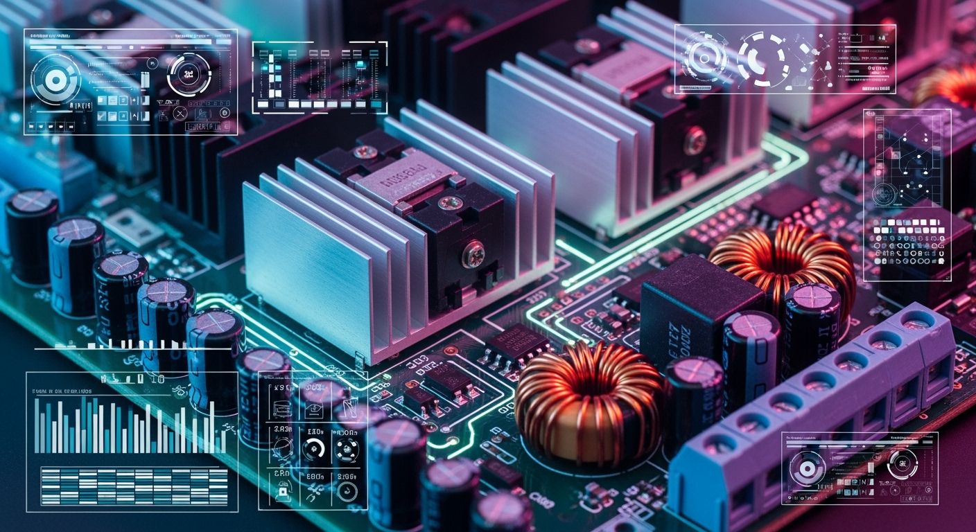
You build strong industrial motor drives to handle quick current changes and high heat release. Modern high-voltage switching parts create intense high-frequency noise inside high-power equipment. You must balance power stage performance with clear feedback signals across sensitive control loops. Whether you build an electric vehicle charger or high-precision motion applications, successful hardware deployment requires expert pcb design for power electronics. Developing a reliable servo drive pcba demands smart substrate selection, low-inductance trace layout, galvanic isolation, and strict EMC testing. Careful board engineering protects sensitive control logic and ensures stable long-term operation across all power electronic systems under heavy operating loads.
Key Takeaways
Choose high-Tg FR-4 or metal core boards to manage strong heat safely.
Put capacitors right beside switches to lower electrical noise.
Keep high-voltage power lines away from control circuits to stop dangerous short circuits.
Put copper-filled thermal vias beneath switches to pull away harmful heat.
Follow IPC guidelines and check circuit boards to make sure the machines stay safe for a long time.
Substrate Selection for Servo Drive PCBA
High-Tg FR-4 vs Metal Core Boards
You must choose base materials carefully to build a reliable servo drive pcba. Strong circuit boards are required for high power electronics. Standard FR4 laminate has a glass transition temperature (Tg) of 130–140°C and runs steadily at 50–115°C. Continuous motor operation creates intense heat under heavy switching loads. High-power motor control systems need board materials with better heat resistance. High-Tg FR4 offers a Tg limit of 170°C or 180°C. This material option allows high-power pcb designs in industrial drives to run steadily at 100–125°C.
Material Type | Glass Transition Temperature (Tg) | Continuous Operating Range |
|---|---|---|
Traditional FR4 | 130–140°C | 50–115°C |
High-Tg FR4 | 170°C or higher | 100–125°C |
Metal core boards move heat away from power switches faster than basic laminates in simple power modules. Multi-layer high-Tg FR4 boards handle complex power signal paths and control logic better while keeping system performance high. You get superior mechanical stability near external heat sinks when surrounding temperatures change quickly. This board design choice stops pcb laminate layers from separating under heavy thermal stress.
Copper Thickness and CTI Ratings
Thick copper layers raise current capacity across high-voltage power traces. You must route high currents and power signals safely without overheating the copper board tracks. Standard pcb designs use thin copper foils for basic digital logic circuits. High-power applications of pcb for power electronics use thicker copper planes to drop electrical resistance and heat buildup. Proper current routing keeps operating temperatures low and extends total hardware service life.
Comparative Tracking Index (CTI) tests how well substrate insulation resists electrical breakdown under high voltage stress. High CTI ratings stop electrical treeing across narrow trace gaps in tight layouts. You protect sensitive electronics logic from damaging short circuits by making smart material choices. Picking high-grade laminates improves overall board reliability and maintains peak performance during heavy motor acceleration cycles under harsh operating environments.
Power Stage Layout and Gate Driver Routing
Optimizing circuit paths prevents signal distortion in modern power electronics systems. You must place the high-power switching stage strategically to achieve clean voltage delivery and maintain peak drive control. Proper component arrangement creates effective signal paths while reducing thermal stress across sensitive control circuits.
Optimizing Servo Drive PCBA Switching Loops
High switching speeds generate fast current changes inside a servo drive pcba stage. Rapid switching across power switches like MOSFETs or IGBTs creates strong electromagnetic fields. You must design compact physical switching loops to control high-frequency noise and prevent excessive voltage spikes.
Tight loop paths minimize parasitic inductance and improve power efficiency during fast switching events.
To optimize the power stage loop, arrange components along a tight, continuous pathway:
Place high-frequency decoupling capacitors directly across the primary DC bus rails next to the power switches.
Minimize the total loop area formed by the DC bus capacitors, top switches, bottom switches, and return paths.
Route return currents on an adjacent inner pcb layer to enable natural magnetic field cancellation.
Standard high-power electronics boards suffer when long traces form large loop antennas. These wide loops radiate unwanted high-frequency interference into nearby feedback control circuits. Placing ceramic decoupling capacitors close to the power switches provides immediate high-frequency current during turn-on transitions. This localized current supply reduces transient voltage dips on the main high-voltage bus. Furthermore, wide surface-mount copper traces enhance the continuous current capacity along high-current paths. Strategic pcb layout practices secure high motor control efficiency while offering excellent noise reduction across all operating modes. Maintaining symmetrical trace routing also balances thermal loads across the board.
Gate Driver Placement and Trace Isolation
Gate driver integrated circuits control the turn-on and turn-off actions of power semiconductors. You must position gate drivers immediately adjacent to power switches like SiC devices or IGBTs. Short gate driver traces minimize parasitic trace inductance. This close placement eliminates gate voltage ringing during rapid high-frequency switching transitions. Low-inductance layout techniques further protect these control circuits from noise. Keeping gate driver return loops extremely short also prevents false triggering under heavy electrical stress.
You must isolate sensitive gate drive traces from high-voltage pcb nodes and high-current power traces. Fast voltage changes on power nodes can inject current into gate traces through parasitic capacitance. Route gate drive signals as differential pairs directly to the gate and source connections of the switch. Keep these traces on an inner layer or shield them with ground guard traces when possible. Cross power traces at perpendicular angles if signals must intersect on adjacent board layers.
Power stage grounds carry massive high-frequency current pulses back to the main supply source. Low-noise analog and digital logic grounds require clean electrical conditions to maintain exact motor feedback performance. You must physically separate high-power grounds from sensitive logic grounds on the pcb. Connect these two distinct ground domains at a single quiet reference point, typically near the current sensing amplifier ground pin. This star-grounding technique prevents heavy power switching currents from polluting delicate sensor readings, which protects overall motor control performance and stops signal degradation across complex high-voltage electronics hardware.
High-Voltage Creepage and Clearance
Smart high-voltage electronics layout uses proper board spacing to stop sparks from jumping across open spaces. You must keep enough physical distance between high-energy traces and weak low-power circuits. Proper spacing prevents sudden short circuits, protects working stability, and keeps equipment safe for user touch.
IEC 61800-5-1 Spacing Rules
Standard IEC 61800-5-1 sets strict safety rules for motor drive systems. You calculate clearance through air and creepage along insulating pcb surfaces based on voltage levels, elevation, and dirt exposure.
Protection Method | Effect on Creepage Requirements | Relevance to High-Voltage Servo Drive PCBA |
|---|---|---|
Conformal coating | Boosts surface insulation and blocks dirt; certified coatings can drop needed creepage by 25-50%. | Lets designers place high-voltage servo drive wires closer together while keeping things safe. |
Potting compound | Covers the full PCBA, an action often needed for Pollution Degree 3 or 4. | Helps servo drives work in dirty or damp areas where higher pollution levels exist. |
Adding a protective conformal layer shields high-voltage wires from damp air. This protective coating drops local pollution levels, letting you safely place traces closer together inside tight power layout zones.
Galvanic Isolation and Ground Separation
Galvanic isolation physically splits high-voltage power paths from low-voltage control loops. You must place optocouplers, digital isolators, or isolated drivers across this line to block high voltage spikes. This physical separation stops noise from messing up delicate sensor circuits during fast motor changes.
Physical isolation lines shield users and weak digital processors from dangerous high-voltage power spikes.
You must keep clean ground lines across the isolated board boundary. Route high-power return paths far away from weak control ground copper. Cutting thin isolation slots straight through inner pcb layers removes electrical tracking paths along dirty board edges. These layout steps stop dangerous current leaks, boost drive stability, and protect long-term signal quality inside tough industrial jobs.
Power Electronics Thermal Management
Heavy electrical loads in industrial drives generate high heat inside modern power electronics. You must dissipate this heat quickly to keep operating temperatures low. Effective heat management strategies shield sensitive control circuits and boost drive efficiency. Smart board construction ensures optimal performance across demanding motor control tasks.
Thermal Via Arrays and Copper Planes
Power switches create localized heat spots during rapid switching events. Surface copper pours spread heat across top layers, but heat must also move down into lower board levels. Thermal resistance measures how strongly a material resists this internal heat flow. You can calculate thermal resistance by dividing temperature difference by total heat flow. Adding dedicated thermal via arrays directly under exposed power switches creates direct conductive paths through the board.
Parameter | Recommended Value | Implementation Notes |
|---|---|---|
Via diameter | ~0.3 mm | Balances heat conduction with board fabrication yield |
Via pitch | ~1 mm | Dense placement directly under the primary heat source |
Plating thickness | ≥25 μm | Wall copper thickness drives vertical thermal conduction |
Via fill | Conductive epoxy resin | Prevents solder wicking and lowers overall thermal resistance |
For boards thicker than 0.7 mm, placing filled vias directly under a thermal pad can reduce thermal resistance by up to 20% compared with unfilled vias.
Using copper-filled via arrays lowers overall board temperature by 22°C compared to unfilled vias. Thicker internal copper planes help move heat away from high-power switches across larger surface areas. Short connections between power devices and ground copper planes keep heat paths simple. Solid heat routing stops hot spots from damaging high-power component solder joints over time.
Heat Sink Integration and TIM Selection
Air cooling along plain pcb layers often fails to cool high-power motor drives under continuous full load. You must mount external heat sinks onto board assemblies to clear massive heat loads. Thermal interface materials fill tiny air gaps between component tops and metallic heat sinks. Selecting proper materials ensures continuous contact and boosts total thermal performance.
Mounting Approach | Mechanical Limit / Guidance | Strain and Load Impact |
|---|---|---|
Spring screws | 20–50 psi contact pressure | Limits board strain to ≤500 μstrain to protect components |
Push-pin mounts | 10–50 psi compressive load | Delivers even pressure across surface-mount packages |
Center-loaded clip | Force centered over package | Minimizes torque variations and protects solder joints |
Careless attachment of heavy metal heat sinks creates mechanical stress across surface-mount packages. High mechanical stress causes invisible cracks inside delicate ceramic parts and solder joints. Spring screws maintain 20–50 psi contact pressure while keeping structural board strain below 500 μstrain. Push-pin hardware applies a steady 10–50 psi compressive load over surface-mount component bodies. Center-loaded clip mounts target clamping force over package centers to reduce stress caused by improper screw torque.
Proper heat sinks draw heat away from active switching circuits smoothly. Mounting rigid heat sinks with controlled clamping force prevents board flexure during thermal expansion. Secure heat sinks shield board components from continuous mechanical vibration in tough industrial sites. Smart layout choices position heavy heat sinks without crowding nearby logic circuits. Matching suitable thermal materials with rugged heat sinks extends system operating life under harsh conditions.
EMI Suppression and Circuit Protection
Strong motor control boards create a lot of electrical noise when running. You need to guard control circuits from sudden high-voltage spikes while lowering electrical noise. Smart board design stops noise where it starts and shields weak parts from bad signals.
Snubber Circuits and Output Filters
Fast part actions make voltage shake back and forth across motor wires. You can put small parts across switches to soak up extra high-voltage energy. Putting special plastic or ceramic parts between 1 nF and 500 nF calms down quick voltage changes during fast motor moves. Picking good parts stops board damage and keeps energy efficiency above 97%.
Evaluation Band / Parameter | Standard Frequency / Value Range | Engineering Relevance |
|---|---|---|
AC Conducted Emission Band | 150 kHz – 30 MHz | Standard testing range for power port emissions |
Common-Mode Noise Peak | Up to 1 MHz | Primary noise range from switching and leakage current |
High-Frequency Leakage Analysis | Up to 1.5 MHz | Evaluates leakage current across long drive cables |
Extra cleanup parts put near power supply lines clean up line noise in modern hardware. Regular tests check power input wires between 150 kHz and 30 MHz. Fast motor switching makes shared line noise that fills up the area below 1 MHz. You can make simple parts to block leaked energy up to 1.5 MHz. These extra parts help drives run better and pass official rules for factory jobs.
Overcurrent and Overvoltage Protection
Big power paths and high-voltage parts need super fast safety circuits to block short circuits. You must track current loads using quick sensing parts or special magnetic chips. These magnetic chips send safe reading signals back to control parts. When current gets too high, safety circuits shut off power parts right away to stop full damage.
Unplanned wire unplugs make tall voltage spikes jump across main power lines. You can hook up safety diodes across main wires to hold down sudden power jumps. Smart board layouts put wide metal traces near fast switches. Heavy copper tracks soak up extra heat during bad line faults. These safety steps keep your circuit board safe from high-voltage sparks and help machines run fine inside factory spaces.
Industry Standards and Design Validation
Making strong motor drives requires following global safety and engineering rules. You must use proven factory methods to stop your circuit board from breaking early. Creating power electronics circuit boards takes accurate wire sizing to carry heavy electrical loads.
IPC Standards for High Power PCBs
You need to pick the right building rules when making tough hardware. The basic IPC-2221 guide gives early layout advice for simple wire sizing. However, you should use IPC-2152 rules to find exact power capacity for heavy electrical uses.
The design rule is to use IPC-2221 for early trace sizing to prevent hot spots, but follow IPC-2152 for modern power charts so wires handle peak motor power safely.
Standard | Role for high-current PCB trace design |
|---|---|
IPC-2221 | Generic PCB design standard covering layout rules, including older conductor current-carrying capacity charts. |
IPC-2152 | Dedicated standard for determining current-carrying capacity in printed board design, used for sizing copper cross-section. |
FCC Part 15 Subpart B / IEC 61800-3 | EMC compliance references for commercial deployment; applicability depends on market, classification, and end use. |
For example, a 10 A trace on thick copper needs a width of at least 100 mil to stay cool. According to IPC-6012 rules, tough factory electronics need IPC Class 3 quality levels. Class 3 needs thicker hole-wall copper plating than Class 2. This extra metal layer protects long-term wire links under heavy physical strain.
Reliability Testing and Thermal Validation
You test board strength by putting parts through tough temperature tests. Micro-section testing checks hidden copper bonds across all high-voltage layers. You must build small test boards to check build quality before main factory production.
Use D coupons to run 6 reflow simulations and 100 thermal shocks.
Measure loop electrical resistance continuously during high-frequency heating tests.
Watch for a resistance rise above 10% to spot early via failures.
Passing 300 to 500 heat cycles shows strong inner copper wall quality. Thorough heat testing finds hot spots before final machine setup. Testing boards under high operating power shields weak control logic from sharp electrical noise. These complete testing steps guarantee top performance inside challenging high-voltage machines.
Building a strong servo drive pcba takes three main engineering steps. You need to combine tight trace layouts, solid high-voltage separation, and clear heat dissipation paths. These smart design choices guard weak control circuits from high-frequency current spikes.
Always run heat models and noise simulations early in the design phase. Testing your layout before setting the pcb stackup stops costly board redesigns in high-power setups. Early testing ensures stable long-term operation under heavy switching loads.
Engineers must follow official IPC and IEC rules during the final testing phase. Sticking to these standard industry rules boosts drive efficiency, improves system voltage control, and guarantees top power performance.
FAQ
Why do high-power solar inverters need high-Tg FR-4 materials?
You need high-Tg FR-4 so solar inverters can take heavy heat stress. High heat happens when continuous power flows through system parts. The material stops layer separation and keeps system performance reliable during high-power use.
How do heat sinks improve cooling in motor systems?
You mount heat sinks right onto the board to draw heat from fast switches. Proper thermal interface materials fill tiny air gaps between parts. Good cooling protects industrial motor drives from extreme heat buildup during long operation.
What reduces high-frequency noise in battery power units?
You cut electrical noise in an electric vehicle charger by placing capacitors close to high-voltage switches. Compact switching loops limit high-frequency current spikes. This clean pcb layout protects sensitive power electronics logic.
Where do green energy systems use high-voltage layout rules?
You build high-power solar units using strong heat sinks for extra cooling. High-voltage traces need strict spacing under standard IPC rules. These smart electronics design steps protect your servo drive pcba in tough system applications.
See Also
Essential Strategies For Sourcing Electronic Components In PCBA Manufacturing
Understanding What The Term PCBA Means In Modern Electronics
A Complete Guide To Choosing The Best PCBA Supplier
