QFN vs QFP Packages: Differences and Applications
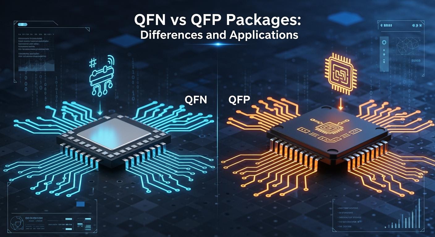
When designing electronics, you often need to choose between QFN vs QFP packages. The primary distinction lies in their lead structure. QFN packages utilize leadless bottom-pad connections, while QFP packages feature gull-wing leads on all four sides. This difference affects how you assemble and inspect each package. Selecting the appropriate package can enhance the reliability and cost-effectiveness of your design. Many engineers prefer QFN packages for high-volume production. For instance:
QFN packages are projected to capture 60% of the market by 2025.
Over half of smartphones incorporate plastic-molded QFN packages.
Consumer electronics are expected to account for about 40% of the QFN packaging market revenue in 2025.
You can observe some key differences in the table below:
Feature | QFN | QFP |
|---|---|---|
Leads | Leadless bottom-pad connections | Gull-wing (L-shaped) leads on all 4 sides |
Assembly | Bottom-side soldering | Easier handling with extended leads |
Pin Count | Varies by package size | 8-70 pins per side (QFP32, QFP64, etc.) |
Understanding these features is essential for selecting the best package for your project, especially when considering QFN vs QFP packages.
Key Takeaways
QFN packages are small and save space. They work well in small devices like smartphones and wearables.
QFP packages are easier to check and fix because you can see their leads. This makes them good for testing and making a few products.
Pick QFN for high-frequency uses because it works better with electricity and heat.
Pick QFP if your project needs more pins and is easier to put together and test.
Knowing the differences between QFN and QFP can help your designs work better and cost less.
QFN vs QFP Packages: Main Differences
Lead Structure and Size
When you compare qfn and qfp packages, look at the lead structure. Qfp connects to the board with gull-wing leads on all sides. Qfn connects with leadless contacts on the bottom. This changes the size and layout of your board.
Here is a table that shows the differences:
Package Type | Lead Configuration | Advantages | Disadvantages |
|---|---|---|---|
QFN | Leadless contacts through bottom-side pads | Reduces unwanted electrical effects, helps high-frequency work | Harder to check visually |
QFP | Gull-wing leads protruding outward | Easier to solder and inspect visually | More unwanted electrical effects |
Qfp packages take up more space because of their leads. You need a bigger board for qfp. Qfn packages are much smaller, about 40% to 60% less space. Qfn is good for small or thin devices. If you want to save space, qfn is a smart choice.
Inspection and Rework
It is easier to inspect and fix qfp packages. The gull-wing leads are easy to see. You can check the solder joints with your eyes or a simple microscope. If you need to fix something, you can remove and replace qfp with basic tools.
Qfn packages are different. The solder joints are under the package. You cannot see them without special equipment. Here are some problems with qfn:
Solder joints are hidden, so you cannot use regular inspection.
You need X-ray or Automated X-ray Inspection (AXI) to find issues.
Inspection costs more because of special tools.
Fixing qfn is hard and needs skilled workers.
A table shows how qfp and qfn compare for fixing:
Feature | QFP (Quad Flat Package) | QFN (Quad Flat No-Lead) |
|---|---|---|
Reworkability | Easy | Difficult |
If you want easy inspection and fixing, qfp is the best choice.
Thermal and Electrical Performance
Thermal and electrical performance matter for every ic package. Qfn and qfp are very different here. Qfn is compact. The bottom pad helps heat move away fast. Qfn has lower thermal resistance, so it manages heat well in small devices.
Qfp has higher standoff height. It can handle more thermal cycles, sometimes over 10,000 cycles. This makes qfp reliable when temperatures change a lot. But qfp has higher thermal resistance and average thermal performance compared to qfn.
Here is a table to compare thermal performance:
Package Type | Thermal Cycling Performance | Reliability | Standoff Height |
|---|---|---|---|
QFN | 1,000-3,000 cycles | Can get solder fatigue | Lower |
QFP | Over 10,000 cycles | Reliable with temperature changes | Higher |
Electrical performance is important too. Qfn has short electrical paths. This lowers lead inductance and resistance. You get better signal quality and less loss at high frequencies. Qfp has longer leads. This can cause more unwanted effects and lower performance in fast circuits.
Here is a table to compare electrical performance:
Parameter | QFP Package | QFN Package |
|---|---|---|
Lead Inductance | 2-5nH per pin | Less than 1nH per pin |
Lead Resistance | Higher (longer path) | Lower (shorter path) |
Parasitic Capacitance | Higher | Lower |
Frequency Performance | Good to 100-200MHz | Excellent to 1GHz+ |
If you need strong heat management and high electrical performance, qfn is best. If you need reliability with changing temperatures, qfp works well.
Application Suitability
Pick the package that fits your project. Qfp and qfn packages are used for different things. Qfp is common in microcontrollers, digital signal processors, and industrial equipment. You can use qfp for testing and small batch production. The leads make it easy to test and fix.
Qfn is popular in consumer electronics, cars, and IoT devices. You find qfn in smartphones and wearables because it saves space and handles heat well. Qfn is also good for power management ICs and high-frequency modules.
Here is a table to help you choose:
Application Area | QFP (Quad Flat Package) | QFN (Quad Flat No-Lead) |
|---|---|---|
Microcontrollers (MCUs) | Used a lot, easy to fix | Less common, good for small designs |
DSPs & Communication ICs | Good for testing | Good for high-frequency or small modules |
Consumer Electronics | Medium-density boards | Good for small devices like phones |
Industrial Control | Stable, easy to inspect | Compact, good for heat |
Power Management ICs | Moderate heat handling | Great for heat performance |
Embedded Systems | Testing & small batch | High-density, needs strong performance |
You can see that qfp and qfn are used in different ways. Qfp is best for easy handling and testing. Qfn is best for small, high-performance products.
Tip: If you design for portable, thin, or high-frequency devices, qfn gives you the most benefits. If you need easy inspection and fixing, or you work with testing, qfp is the better choice.
What is QFP?
QFP Structure
QFP stands for Quad Flat Package. It has a flat body that is square or rectangle. There are leads on each side of the package. These leads bend outward and look like gull wings. The gull-wing shape helps you solder the QFP to a circuit board. You can see the solder joints with your eyes or a microscope. This makes it easy to spot problems fast.
The way a QFP is built changes how it works and lasts. The table below shows how parts of the QFP affect its performance and reliability:
Structural Characteristic | Impact on Performance and Reliability |
|---|---|
Gull-wing leads | You can inspect and fix them easily after assembly |
Connection method | Longer leads can change how signals travel |
Thermal behavior | Leads help move heat away and manage temperature |
QFP packages use longer leads. This can change how signals move inside the device. The leads also help heat leave the chip, which keeps it safe.
Common Features
QFP packages have many features that make them popular. Most have a flat surface and leads on all sides. The number of pins can be from 32 to 304. This means you can use them for many kinds of circuits. The space between pins, called pitch, is usually between 0.4 mm and 1.0 mm. This gives you choices when you design your board.
The table below lists common features you will find in QFP packages:
Feature | Description |
|---|---|
Package Type | Flat, square or rectangle with leads on four sides. |
Pin Count | From 32 to 304 pins for different uses. |
Pitch Distance | Usually 0.4 mm to 1.0 mm, so you can design boards easily. |
Lead Shape | Gull-wing shape gives support and strong soldering. |
Material | Made from plastic, ceramic, or metal; leads coated with gold, silver, copper, or tin. |
Applications | Used in electronics, communication gear, microprocessors, and power circuits. |
Challenges | Small pins and close pitch can break; you must handle and design boards carefully. |
QFP packages give you lots of connections and work well in medium and high-frequency circuits. You need to be careful because small pins can bend or break. You should design your circuit board carefully when using QFP. You will see QFP packages in computers, phones, and machines.
Note: QFP packages are easy to inspect, have strong connections, and let you design in many ways. You can use them in lots of projects, but always handle them with care.
What is QFN?
QFN Structure
You may see the term QFN when you look at modern electronics. QFN stands for quad flat no-lead. This package has a flat, square body with no leads sticking out from the sides. Instead, the qfn package uses metal pads on the bottom. These pads connect directly to the circuit board. You get a strong and reliable connection with this design.
The qfn package often includes a large pad in the center. This pad helps move heat away from the chip. You can use this feature to keep your device cool. The small size of the quad flat no-lead package makes it perfect for thin and compact products. You will find that the qfn package fits well in devices where space matters.
The history of the qfn package goes back to early work on high-frequency technology. In 1897, J.C. Bose showed how circuits could work at very high frequencies, up to 60 GHz. This research helped engineers create new ways to build smaller and faster packages. Over time, the qfn package became popular because it supports high-speed and high-frequency circuits.
Common Features
You will notice several features when you use a qfn package. The most important is the leadless design. This means you do not see any leads on the sides. The metal pads on the bottom make assembly easy and save space on your board.
Here are some common features of the quad flat no-lead package:
Very low profile and small footprint
Metal pads on the bottom for electrical and thermal contact
Central thermal pad for better heat dissipation
Good electrical performance at high frequencies
Simple shape for easy placement by machines
Feature | Description |
|---|---|
Body Shape | Flat, square, or rectangular |
Lead Type | No leads on sides, only bottom pads |
Thermal Pad | Large pad in center for heat transfer |
Pin Count | Usually 8 to 64 pins, sometimes more |
Application | Used in phones, wearables, and IoT devices |
You can use the qfn package in many products. The quad flat no-lead design helps you build smaller, lighter, and faster devices. You also get better heat management and strong electrical signals. The qfn package gives you a modern solution for today’s electronics.
QFP vs QFN: Side-by-Side Comparison
Difference Between QFP and QFN
You can spot differences between qfp and qfn easily. Both are surface mount types, but their designs are not the same. Qfp has gull-wing leads sticking out from all four sides. Qfn does not have leads on the sides. Qfn uses metal pads under the package. This makes qfn smaller and lighter.
Here is a table to show the main differences:
Feature | QFP (Quad Flat Package) | QFN (Quad Flat No-lead) |
|---|---|---|
Lead | Gull-wing leads extend outwards | Metalized contacts underneath, no side leads |
Assembly | Excellent footing, self-aligns during assembly | Average footing, needs careful placement |
Pin Count | 32 to 280 pins or more | Usually 8 pins plus a thermal pad |
Qfp is good for projects needing lots of connections. Qfn is best for small devices where space is important.
Assembly and Soldering
You should know how assembly and soldering are different for each package. Qfp is easier to assemble because you can see and touch the leads. You can check the solder joints with your eyes or a microscope. Qfn hides the solder joints under the package. You need special tools to check them.
Here is a table showing assembly and soldering differences:
Feature | QFP (Quad Flat Package) | QFN (Quad Flat No-lead) |
|---|---|---|
Pin Accessibility | Easy to see and solder by hand | Solder surfaces on underside, hard to see |
Solder Joint Visibility | Simple to inspect | Difficult to inspect |
Center Ground Requirement | Not required | Needs center ground soldering for heat |
Cleaning | Easy to clean | Harder to clean |
Cold Solder Joint Issues | Less likely | More likely due to hidden joints |
Qfp is a good choice if you want easy assembly and repair. Qfn is smaller but needs more care during assembly.
PCB Design Impact
You need to think about how each package changes your PCB design. Qfp takes up more space because of its leads. Qfn lets you make smaller boards since it has no side leads. Both work well with machines for surface mount assembly.
Here is a table for quick comparison:
Aspect | QFP Package | QFN Package |
|---|---|---|
Size | Larger than qfn | Smaller, saves board space |
PCB Size Impact | May need a bigger board | Allows for smaller board |
Assembly Complexity | Works well with machines | Works well with machines |
Soldering/Rework Ease | Easy to solder or fix by hand | Needs reflow oven for rework |
Cost Consideration | Uses more solder in big orders | Smaller board can lower costs |
Testing/Verification | Standard testing | Needs extra steps for testing |
Qfp makes prototyping and repairs simple. Qfn helps you save space and lower costs, but you need special inspection and rework steps.
Tip: Pick qfp if you want easy handling and testing. Choose qfn if you need a compact, high-performance surface mount package.
Choosing QFN or QFP
When to Use QFN
Pick a qfn package if your project needs to be small. Qfn is great for devices with little space. It helps manage heat well and works at high frequencies. Engineers use qfn in smartphones, wearables, and IoT devices. Qfn packages move heat away quickly and keep signals strong. If your board handles fast or RF signals, qfn works best. Factories like qfn because it uses less material and costs less.
Here is a table to help you choose:
Factor | QFN |
|---|---|
PCB Space | 30-50% smaller footprint |
Thermal Performance | Superior heat transfer |
Pin Count | Lower pin count |
Inspection | Needs X-ray or advanced methods |
Application | High-speed, RF signals |
Manufacturing | Automated production preferred |
Cost | Cost-sensitive, high volume |
Tip: Pick qfn if you want a small board, good heat control, and strong performance at high frequencies.
When to Use QFP
Choose a qfp package if you need easy checking and fixing. Qfp is good for testing and making a few boards. You can see and fix the leads without special tools. If your design needs lots of pins, qfp gives more choices. Engineers use qfp for microcontrollers, industrial controls, and communication systems. Qfp makes building and fixing simple.
Here is a table to help you decide:
Factor | QFP |
|---|---|
PCB Space | More space available |
Thermal Performance | Moderate thermal requirements |
Pin Count | Higher pin count, up to 300+ pins |
Inspection | Easy visual inspection and rework |
Application | Prototyping, low-volume builds |
Manufacturing | Simpler manufacturing and debugging |
Cost | Reduced development risk |
Note: Pick qfp if you want easy handling, lots of pins, and simple repairs.
Industry Examples
You see qfn and qfp packages in many industries. Consumer electronics use qfn in phones and fitness trackers. Cars use qfn for small sensors and power chips. Factories use qfp for microcontrollers and signal chips. Communication devices use qfp for chips with many pins. Wearables and IoT products use qfn because it saves space and handles heat well.
Qfn is used in phones, wearables, and RF modules.
Qfp is used in industrial controls, test boards, and communication systems.
You can pick the package that fits your project. Qfn is good for small, fast devices. Qfp is good for bigger boards that need easy fixing.
You can easily tell QFN and QFP packages apart. The table below shows the main differences:
Feature | QFN (Quad Flat No-lead) | QFP (Quad Flat Package) |
|---|---|---|
Size | Smaller, saves PCB space | Larger, needs more board area |
Thermal Handling | Excellent, exposed pad | Moderate, uses leads |
Assembly | Needs precision, harder rework | Easier to inspect and repair |
QFN is great for small and fast devices. QFP is better if you need to check or fix things easily, or if your project needs lots of pins. Always pick the package that fits your project, your building skills, and what is popular in electronics.
FAQ
What is the main difference between QFN and QFP packages?
You see QFN packages with no leads on the sides. QFP packages have gull-wing leads. QFN saves space. QFP makes inspection and repair easier.
Can you solder QFN packages by hand?
You can solder QFN by hand, but it is tricky. The pads sit under the package. You need a hot air tool or reflow oven for best results.
Which package is better for high-frequency circuits?
QFN works best for high-frequency circuits. The short electrical paths reduce signal loss. You get better performance in RF and fast digital designs.
How do you inspect solder joints on QFN packages?
You cannot see QFN solder joints with your eyes. You need X-ray inspection or special machines. QFP joints are easy to check visually.
Are QFP packages good for prototyping?
QFP packages help you with prototyping. The leads are easy to solder and fix. You can test and change your design without special tools.
See Also
Understanding SMT And DIP Assembly In PCBA Processes
Double-Sided Reflow Soldering Techniques For PCBA Manufacturing
Comparing Stacked And Staggered Microvias In PCB Design
