Breaking Down the SMT Assembly Process into Key Steps
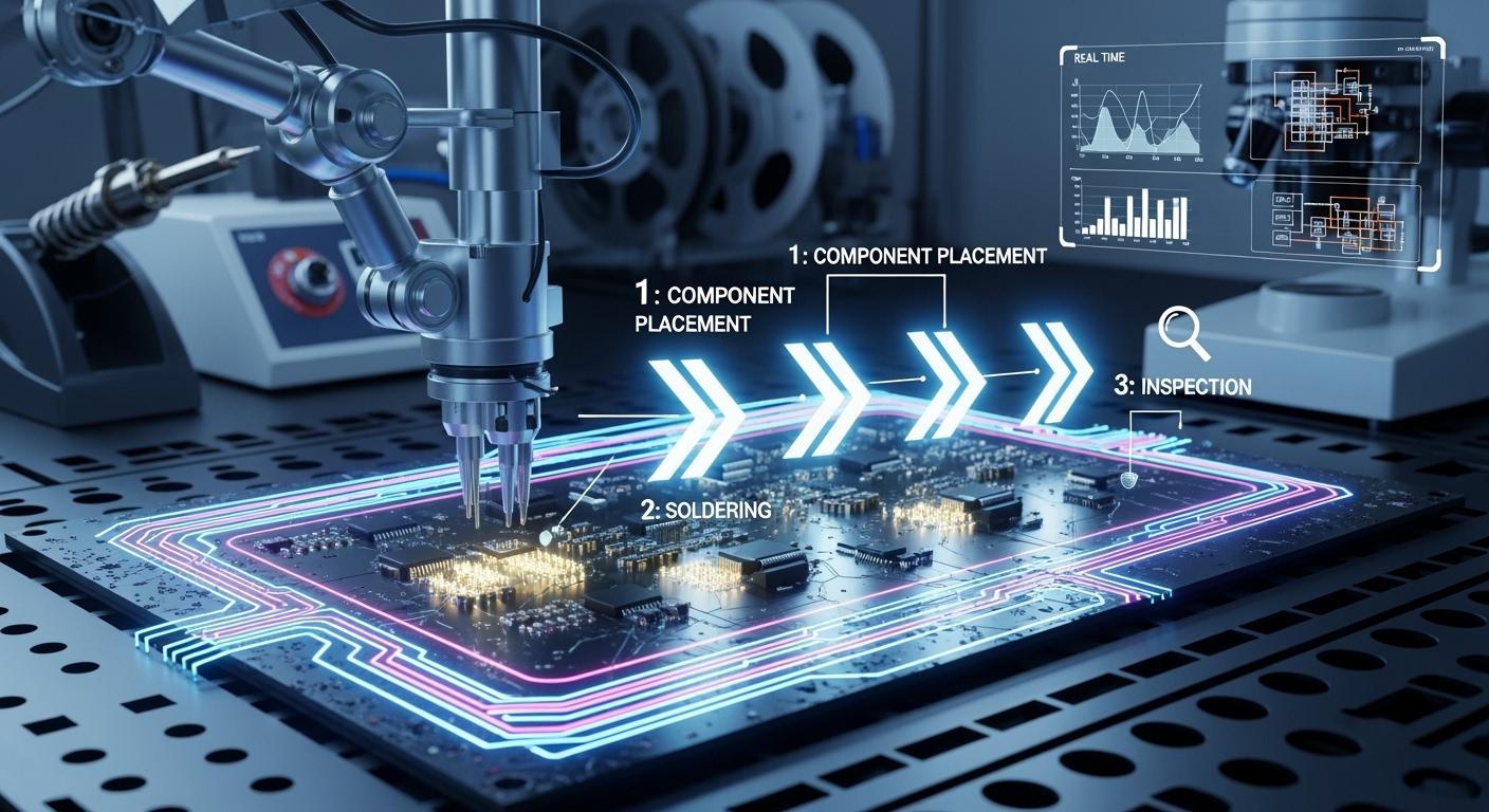
You go through many important steps in the smt assembly process. These steps are pre-production preparation, solder paste application, solder paste inspection, component placement, visual inspection, reflow soldering, post-reflow inspection, and final testing. Knowing what happens at each stage helps you get good surface mount technology results.
Doing these steps carefully lowers mistakes and makes devices last longer.
Putting solder paste the same way each time and placing parts correctly helps make strong solder joints.
Following rules closely and keeping equipment in good shape makes assemblies work well.
Key Takeaways
Go through each step of the SMT assembly process slowly to make fewer mistakes and help products work better.
Use machines like AOI and X-ray to find problems early, so the boards are good quality.
Take care of the machines and put on solder paste the same way each time to make strong solder joints.
Test the PCB well to make sure it works right before you send it out.
Use DFM and DFA ideas to make designs better and have fewer mistakes when making things.
SMT Assembly Process Flow Overview
What Is Surface Mount Technology?
You use surface mount technology to build modern electronic devices. This method lets you place electronic parts directly onto the surface of a printed circuit board (PCB). You do not need to drill holes for each part, which saves time and space. Surface mount technology helps you make smaller and lighter products. You can fit more components on a single board, which is important for phones, computers, and other portable devices. You also get better reliability because the connections are strong and less likely to break. Automation makes the process faster and reduces mistakes, so you can produce more devices at a lower cost.
Tip: Surface mount technology works best when you want to make many devices quickly and keep them small and reliable.
Key Steps in the SMT Assembly Process
You follow a clear smt assembly process flow to build high-quality electronics. Each step connects to the next, making sure your final product works well. Here are the main stages you will see in the smt assembly process flow:
Solder Paste Application: You apply solder paste to the PCB using a stencil. This step prepares the board for parts.
Component Placement: You use machines to place each part on the board. The machines work fast and keep parts in the right spot.
Reflow Soldering: You heat the board in a special oven. The solder paste melts and connects the parts to the board.
Inspection and Testing: You check the board for mistakes. You use machines or manual checks to find problems and make sure everything works.
You can improve each step by keeping your equipment in good shape and training your team. Real-time monitoring and regular checks help you catch problems early. When you follow these steps, you get strong, reliable boards that last a long time.
Pre-Production Preparation
DFM and DFA Analysis
You begin the pcb smt assembly process by checking your design. Design for manufacturability (DFM) and design for assembly (DFA) help you make smart choices. These methods link your design to what manufacturing can do. Using DFM and DFA lets you spot problems early. You avoid expensive mistakes. You get more boards right the first time. Lead times get shorter. Your bill of materials stays steady. You spend less money overall. Your team learns from real production data and improves designs.
Note: DFM and DFA can raise yield by 5-20 percentage points. They can lower defect rates by up to 30%. You see fewer mistakes and stronger boards.
Improvement Type | Percentage Improvement |
|---|---|
Yield Improvement | 5-20 |
Defect Rate Reduction | Up to 30 |
PCB Preparation Steps
You get your PCB ready before assembly starts. You gather and check customer documents like Gerber files, BOM, and pick & place coordinates. Gerber files must have copper layers, drill files, and process edges. BOMs need reference designators, part numbers, and packaging types. Pick & place files should show X/Y positions, rotation angles, and package types. You also look for special needs, like temperature-sensitive parts or special solder paste.
You check incoming materials. You look at part numbers, packaging, and moisture levels. You reform and tape materials so they fit SMT feeders. You bake moisture-sensitive parts to stop defects. You load and check feeders to make sure parts are in the right spot and facing the right way.
Tip: Careful preparation helps you avoid delays. It makes sure your pcb smt assembly services give reliable results.
Solder Paste Application
Solder paste application is a key step in the SMT assembly process. You use this step to put small amounts of solder paste on the pads of your printed circuit board. The paste holds the components in place before you heat the board. If you do this step well, you get strong and reliable solder joints. Most soldering problems start here, so you need to pay close attention.
Stencil Printing Process
You use a stencil printer to apply the solder paste. The stencil is a thin metal sheet with holes that match the pads on your PCB. You place the stencil over the board. A squeegee pushes the paste across the stencil, filling each hole. When you lift the stencil, the paste stays on the pads in the right shape and size. You must choose the right stencil thickness and hole size for your components. If you use the wrong size, you may get too much or too little paste. This can cause weak joints or bridges between pads.
Tip: Clean your stencil every 10 to 20 prints. This stops paste buildup and keeps your prints sharp.
Best Practices for Solder Paste Application
You can improve your results by following these best practices:
Match the stencil thickness and hole shape to your smallest pad size.
Keep the squeegee speed and pressure steady. This helps you avoid smears and skips.
Control the room temperature and humidity. Solder paste works best in stable conditions.
Check the solder paste often. Measure the height, volume, and area to keep it consistent.
Store your paste in the right way. Old or warm paste can cause defects.
Use automated inspection after printing. This checks if the paste is in the right place and amount.
You lower the risk of defects when you follow these steps. You also make sure you get high-quality smt solder paste results. Careful solder paste application helps you build strong and reliable boards every time.
Solder Paste Inspection (SPI)
Purpose of SPI
You need to check the solder paste right after you print it on the PCB. Solder Paste Inspection (SPI) helps you spot problems early. Most SMT assembly defects—about 60–80%—come from poor solder paste printing. Common issues include not enough paste, too much paste, or bridges between pads. If you catch these mistakes now, you avoid bigger problems later.
SPI gives you more than just a quick check. It lets you use data to adjust your printer settings automatically. This closed-loop control keeps your print quality steady during the whole run. You get better yields, less rework, and stronger boards. When you use SPI, you save time and money because you fix problems before they move down the line.
Tip: SPI can reduce your defect rate by over 90% when you combine it with other inspection tools like AOI and X-ray.
Common SPI Methods
You have several ways to inspect solder paste. Each method fits different needs and budgets. Here is a table to help you compare them:
Method | Advantages | Limitations | Best Use Case |
|---|---|---|---|
Manual Visual Inspection | Low cost, no extra tools needed. | High chance of missing errors, slow, people get tired. | Small batches or simple boards. |
2D Automatic Optical Inspection | Fast, works well on most lines. | Cannot measure paste height or volume, sensitive to light reflections. | General production lines. |
3D Automatic Optical Inspection | Very accurate, measures volume and height, supports feedback control. | Costs more, needs advanced tech. | High-end or critical boards. |
Solder Paste Thickness Gauge | Cheap, easy to use. | Destroys the sample, not good for every board. | Labs or process checks. |
X-Ray Inspection | Sees inside, checks hidden areas, good for complex boards. | Expensive, slow, needs safety steps. | Special cases with multi-layer stencils. |
You get the best results when you use advanced inspection systems. These tools catch defects early and give you real-time feedback. You can fix problems right away, which keeps your boards strong and your process smooth.
Component Placement
Automated Placement Machines
Automated placement machines put parts on your PCB fast and right. These machines pick up each part and set it in the correct place. They can work very quickly and place over 100,000 parts every hour. This speed helps you finish many boards in less time.
Machines can handle very tiny parts that people cannot place well.
They use cameras and sensors to check where each part goes.
You get fewer errors because machines follow exact steps.
Most machines today can place parts with an accuracy of ±0.025mm. This is good enough for 0201 micro-components.
You can trust these machines to keep your work fast and steady. Using them also lowers the chance of mistakes people might make.
Placement Accuracy and Challenges
You need to be very accurate when you place parts. This makes sure your board works as it should. Modern machines can keep accuracy within ±25 microns. This lets you use very small parts and build hard circuits.
You may have some common smt problems during this step:
SMT parts are very small, so they are hard to handle and place. You need good machines to stop parts from falling or going in the wrong spot.
You must be very exact to stop parts from being crooked. Even a small move can make the board not work.
Solder joints must be strong. If they are weak, your board might break. Things like heat, stress, and dirt can hurt the joints.
A good PCB design helps you put parts in the best places. A careful layout makes placement and the board’s work better.
You can fix these problems by keeping machines clean, checking your work often, and teaching your team. If you focus on being exact and designing well, you get strong and steady boards every time.
Visual Inspection
Manual and Automated Visual Checks
You check your PCB for problems after you place parts. This step helps you find mistakes early. It also keeps your boards working well. You can use your eyes or a magnifier for manual inspection. You look for missing parts, crooked pieces, or solder bridges. Manual checks are good for small groups of boards or simple designs.
Automated Optical Inspection (AOI) uses cameras and special software. AOI scans the board for surface problems. It checks if parts are in the right spot and if the polarity is correct. AOI works fast and always checks the same way. It does not get tired or miss small things. You get results you can track and use to make your process better. AOI is great for lines that run all the time. It also lowers mistakes people might make.
AOI systems help you find errors faster and more accurately. You can trust AOI to catch problems and keep your boards good.
Here is a table that shows how inspection methods compare:
Inspection Method | Primary Focus | Common Defects | Speed | Board Suitability | Cost |
|---|---|---|---|---|---|
AOI | Surface and top-side features | Misplacement, polarity, bridges | High (inline capable) | Low to medium density | Lower initial investment |
AXI | Internal and hidden structures | Voids, cracks, via fills | Moderate (offline) | High density, multi-layer | Higher due to equipment |
Identifying Placement Issues
You need to find placement problems before the next step. Visual inspection helps you see parts that are not lined up, wrong polarity, and soldering mistakes. You look for bridges, missing parts, and bent leads. Finding these problems early lets you fix them fast and saves money.
Visual inspection helps you find surface problems quickly.
You make quality better by catching issues early.
Automated checks make finding mistakes faster and more exact.
You keep your boards strong when you use both manual and automated checks. Visual inspection is a cheap way to keep high standards and stop problems before they hurt your final product.
Reflow Soldering
Reflow Oven Process
A reflow oven connects parts to your PCB. The oven heats the board in steps. There are four main zones in the oven. Each zone has a special job to do.
Zone | Purpose |
|---|---|
Preheating Zone | Slowly warms the board to stop damage and cracks. |
Soaking Zone | Keeps the board at one temperature to heat it evenly and start the flux. |
Reflow Zone | Gets very hot so the solder melts and makes strong bonds. |
Cooling Zone | Quickly cools the board to make the joints hard and stop bad compounds. |
The board moves through each zone in the oven. The preheating zone warms the board slowly. This keeps parts from breaking. The soaking zone holds the heat steady. This helps the solder paste spread and the flux work. The reflow zone is the hottest part. Here, the solder melts and connects the parts. The cooling zone cools the board fast. This makes the solder joints hard and stops bad things from forming.
Tip: You can use different heating plans in your oven. The Ramp-Soak-Spike plan changes heat slowly and lowers mistakes. The Ramp-to-Spike plan heats up fast and is good for lead-free solder.
Key Parameters for Quality Soldering
You must control some things to get good solder joints. Each thing you control helps your board work better.
Parameter | Description |
|---|---|
Temperature Profiling | Sets how the oven heats and cools, which changes solder joint quality. |
Stencil Design | The thickness and hole size must fit the pad to stop extra solder and mistakes. |
Printing Parameters | The squeegee’s angle, pressure, and speed change how the paste goes on. |
Solder Paste Properties | How thick and sticky the paste is changes how it spreads and sticks. |
Reflow Process Phases | Preheating, soaking, reflow, and cooling all help make strong joints. |
You set the right heat plan in your oven. This stops the solder from getting too hot or cold. You match the stencil to the pad size. This stops too much solder from making bridges. You check how you print the paste to keep it even. You pick paste that spreads and sticks well. You follow each oven step to make strong and safe joints.
Note: Special heat plans in your oven help with tricky boards. You get better solder joints and fewer problems.
Post-Reflow Inspection
AOI and X-ray Inspection
After reflow soldering, you must check your boards for problems. AOI helps you find surface problems fast. AOI uses cameras and software to scan the board. It looks for misplaced parts, wrong polarity, or solder bridges. AOI works well for most surface issues.
But some problems are hard to see from outside. X-ray inspection lets you look inside the board without taking it apart. You use X-ray to check solder joints inside, especially for BGAs or QFNs. These parts hide their connections under the package. X-ray shows if the solder joints are solid or if there are hidden gaps. You can find problems that AOI or manual checks might miss. This step is important for inspection and quality control. It helps you catch defects before the boards move to the next stage.
AOI is great for surface problems. X-ray inspection is important for finding hidden problems inside the board.
Detecting Soldering Defects
You want to find and fix soldering problems right after reflow. Post-reflow AOI inspection helps you catch many common problems, like:
Solder bridging between pads
Tombstoning, when a part stands up on one end
Component misalignment
Not enough solder on pads
You may also see problems like heat issues, contamination, or mistakes from equipment settings. If the oven is too cool, you get cold joints. If it is too hot, you can hurt parts. Uneven heat can cause tombstoning or weak joints.
You should compare your results with pre-reflow inspection data. This helps you see if problems started before or after reflow. By using both AOI and X-ray, you make sure your boards are good. You keep your process strong and your products reliable.
Final Testing and Quality Control
Functional Testing
Final testing is the last step in the smt assembly process. This step checks if your PCB works the way it should. You use different tests to make sure the board is good.
AOI looks for missing or crooked parts and bad soldering.
X-ray inspection checks hidden joints and how much solder is there, especially for BGAs.
ICT tests each part and connection for shorts or open spots.
Functional testing acts like real life to see if the board works right.
Functional testing helps you find problems early. You check if the board turns on, answers signals, and does what it should. This makes sure your PCB is ready before you send it out. Companies that use AOI can get their first-pass yield from 80% up to over 98%. Some lines say 99.5% of boards pass the first test.
Functional testing and ICT make sure every part works and is in the right spot. You can trust your board to work well when used.
Ensuring Reliability
You want your PCB to last a long time and work well. Inspectors use IPC-A-610 rules to check quality. They look at where parts are, if solder joints are strong, if the board is clean, and if it looks good. You must meet the right class for your product:
IPC Class | Typical Use | Reliability Expectation | Acceptance Strictness |
|---|---|---|---|
Class 1 | General electronic products | Basic function, limited life | Lowest |
Class 2 | Dedicated service electronics | Extended life, steady performance | Medium |
Class 3 | High-reliability electronics | Mission-critical, harsh use | Highest |
You stop common problems by following good steps:
Keep solder paste the right thickness to stop solder balls.
Use AOI to find missing parts and check the BOM.
Watch oven temperature to stop bad soldering and make strong joints.
Handle and store PCBs the right way to stop bending.
You make strong boards when you do these things. Quality control and testing help you give people products that work well and last a long time.
You get good PCB assembly when you follow each smt assembly step carefully. You need to control each step and place parts in the right spot. Checking your work often helps you make strong boards. If you find mistakes early, you can fix them fast. Cleaning the stencil and keeping the squeegee speed steady helps you get better results.
Watch each step closely to stop mistakes.
Use AOI and X-ray to find errors early.
Clean stencils often so you do not get defects.
Practice | Reliability Boost |
|---|---|
Stencil cleaning | Fewer defects, higher yield |
Optimized printing | Strong solder joints |
Surface mount technology helps you follow rules and make products you can trust.
FAQ
What is the main reason for defects in SMT assembly?
You often see defects because of poor solder paste application. If you control the paste thickness and placement, you lower the risk of weak joints and bridges.
How do you choose the right stencil for solder paste?
You match the stencil thickness and hole size to your smallest pad. This helps you get the right amount of paste and avoid extra solder.
Why do you use AOI and X-ray inspection?
AOI finds surface problems fast. X-ray checks hidden joints, especially for BGAs. You use both to catch mistakes early and make your boards reliable.
Can you place tiny components by hand?
You can place small parts by hand for simple boards. Automated machines work better for tiny parts like 0201 chips. Machines give you more accuracy and speed.
What does functional testing check?
You use functional testing to see if your board works as expected. This test checks power, signals, and basic functions before you ship the product.
See Also
Common Techniques and Workflows for SMT Assembly
Understanding SMT and DIP Assembly for PCB Applications
Meeting SMT Assembly Standards for Automotive Manufacturing
Optimizing Hardware Assembly Processes for Improved Outcomes
Top SMT Assembly Techniques for Superior Electronic Production
