DFM Review Process and Guidelines for Hardware Engineers

You stop early risks by checking your design first. This saves money on costly board fixes later. A standard DFM Review Process connects your hardware teams. Easy design for manufacturability checks find big mistakes. You spot flaws before spending money on factory production. A simple review finds bad clearance errors. It also finds bad pcb traces. Smart design for manufacturing rules cut waste costs. They stop costly factory problems. Every good review helps make more working pcb boards. This happens before factory tools are made. A constant DFM Review Process saves you precious time and money.
Key Takeaways
Early DFM reviews find mistakes fast.
They save big factory fix costs.
Smooth outer cases stop plastic flaws.
Good wall thickness keeps parts flat.
Draft angles help plastic parts slide out.
They pop out of molds easily.
Correct PCB trace widths keep boards cool.
Good hole sizes make them reliable.
Complete checklists stop factory delays.
They also reduce total material waste.
Standard DFM Review Process
A step-by-step DFM plan turns ideas into products. Early checks find big design mistakes. You run this process in every build phase.
Architecture Phase and Material Selection
First, you pick your raw materials and parts. Early team checks show progress to everyone. These checks help engineers work well together. They stop sudden design problems later. Teams fix errors before they grow big. You test heat, strength, and power early.
Catching bad materials early saves money. It stops broken parts after machining. Clear views across production catch material flaws quickly. This protects your total product count.
Good materials help you build things easily. They protect your parts and save future work.
CAD Integration and Tooling Feasibility
Modern CAD software makes early checks very easy. You run simple DFM tests inside your software. To help machine parts better, add these automatic rules:
Hole and Thread Specifications: Check hole sizes and screw thread details accurately.
Feature Geometry & Accessibility: Check deep pockets, inside corners, and tool reach.
Surface and Precision Standards: Check surface smooth needs and tight size limits.
These quick checks match your PCB layout to factories. You stop expensive tool fixes before production begins.
Pre-Gerber and Tooling Release Sign-Off
Do one final DFM check before sending files out. This official step reviews every layer and line carefully. You compare your PCB to real factory limits.
Review Focus | Key Checks | Manufacturing Impact |
|---|---|---|
Electrical Rules | Trace gaps, via sizes, board clearance | Stops bad short circuits and open lines |
Mechanical Fit | Tool holes, outer shapes, part heights | Stops parts from hitting outer cases |
A full DFM check verifies all copper lines. The list catches small space errors early. Software finds hidden electrical testing errors fast. Finish this full checklist before final file approval. This strict gate prevents extra costs and factory delays.
Mechanical Enclosure DFM Guidelines
Mechanical housing rules must match real factory needs. You connect hard outer cases to electrical pcb boards. A dfm manufacturing process guides your design choices. Smart decisions protect tiny board parts during final assembly.
Wall Thickness Uniformity and Limits
Uneven walls make bad spots in plastic cases. Keep wall sizes smooth for steady material flow. Plastic cools wrong when wall size changes fast. Temp changes cause ugly flaws and weak spots.
Cosmetic Defects: Bad shrinking leaves sink marks, hesitation marks, lines, burns, and spots.
Structural and Dimensional Defects: Wall shifts cause holes, warps, bends, sizing errors, weak lines, short shots, extra flex, and breaks.
Keep wall sizes in safe ranges for good builds. Connect thin and thick parts with soft slopes. Smooth shapes keep production high in your dfm manufacturing process.
Draft Angles and Feature Ejection
Molded parts need angled sides called draft angles. Angles help parts slide out of metal molds. Good angles form a main part of design for manufacturing.
Keep inner and outer walls parallel in molds. Straight walls remove deep tool ribs. This method opens molds fast, cuts polish time, speeds work, and drops parts easily.
Draw Direction: Use angles along split lines to keep parts on pin sides.
Through-Holes: Angle inside holes toward core sides to stop mold sticking.
Stepped Parting Lines/Shut-offs: Use 5° to 7° angles on touch spots to close mold gaps.
This chart shows small draft angles for depths and wall limits:
Feature Depth | Wall Thickness | Minimum Draft Angle |
|---|---|---|
0.25 in. | 0.040 in. | 0.5° |
0.50 in. | 0.040 in. / 0.060 in. | 1.0° / 0.5° |
0.75 in. | 0.040 in. / 0.060 in. / 0.080 in. | 2.0° / 1.0° / 0.5° |
1.00 in. | 0.060 in. / 0.080 in. / 0.100 in. | 2.0° / 1.0° / 0.5° |
1.50 in. | 0.080 in. / 0.100 in. | 2.0° / 1.0° |
2.00 in. | 0.100 in. | 2.0° |
Small angles stop air from reaching cooling plastic parts. Trapped air creates strong suction that bends parts. Tight friction slows shop work and breaks pcb mounting posts.
Production Metric | Minimal / Zero Draft Condition | Optimized Draft Condition | Operational Impact |
|---|---|---|---|
Ejection Force Spike | Exceeds 10x standard levels (up to 23 metric tons) | Reduced by 60% to 80% via $F = \mu \times N \times A \times \cos(\alpha)$ | Prevents part distortion and tooling overload |
Ejector Pin Wear Rate | 0.03 mm per hour (at 0.5° draft) | 0.01 mm per hour (at 1.5° draft) | 67% reduction in pin degradation |
Ejection Cycle Time | 3.2 seconds | 1.8 seconds | 44% faster cycle performance |
Annual Mold Maintenance | $18,200 / year (without analysis) | $7,800 / year (with analysis) | 57% cost reduction in tool upkeep |
Tiny angles make walls stick hard to molds. Stuck parts delay daily plant build schedules. Forcing stuck parts out causes scratches, twists, or snaps. High friction wears tools out very fast. Run full angle checks in every dfm manufacturing process.
Tolerance Stack-Up and Datums
Strong outer cases must fit pcb setups well. Control size changes with ASME Y14.5 datums.
Align Datums with Physical and Inspection Reality: Pick main datums based on part mounts and test tools.
Trace Datums Through the Assembly Chain: Link datum points through part stacks to main bases.
Perform Datum Shuffles to Match Constraints: Shift datum links when real part fits show surprises.
Utilize Tolerance Analysis Software: Use EZtol or CETOL 6σ to check fits and fix datums.
RSS math gives fast answers for size checks. RSS uses basic rules for good guesses without heavy math in weekly dfm reviews.
Statistical Technique | Recommended Usage | Key Characteristics / Trade-offs |
|---|---|---|
Worst-Case Analysis | Mission-critical assemblies needing 100% fit assurance | Best for low-volume, high-consequence products or chains with few parts. |
Root Sum Square (RSS) | Standard choice (>90% of the time) for quick, realistic evaluations | Delivers swift calculations; ideal for cost-sensitive high-volume manufacturing. |
Good fit checks stop bad pcb hole aligns. Correct datums protect loaded pcb boards from case press damage.
Part Consolidation and Fasteners
Using fewer total parts helps build things fast. Combine small case features right into main moldings.
Apply Three Minimum-Part-Count Criteria: Check if parts move, need unique materials, or split for builds. Merge parts that fail all three checks.
Leverage Complex Manufacturing Technologies:
Injection Molding: Add snap joints and plastic hinges to cut screws.
Die & Investment Casting: Cast cut metal parts into single whole pieces.
Sheet Metal & Extrusions: Use sheet dies to combine mounts into one piece.
Additive Manufacturing: Print multi-part builds as single items without shape limits.
Engineers use design rules to fix connections. John Deere used standard screws and auto-align features. This smart step cut labor, reduced errors, and raised work output.
Snap joints cost less than screws on pcb cases.
Performance / Cost Metric | Snap-Fit Design | Threaded Hardware Fasteners |
|---|---|---|
Structural Integrity & Load Capacity | Lower load limits; unsuitable for severe impacts or heavy loads. | Handles higher shear and tensile forces; provides higher clamping force. |
Component & Material Cost | Zero external hardware costs; simplifies the bill of materials. | Increases expenses by requiring separate screws, nuts, or inserts. |
Manufacturing & Assembly Time | Fast assembly (approx. 2–5 seconds per joint). | Slower assembly process (approx. 15–30 seconds per joint). |
Snap fits hold less weight than strong screws. Yet, snap designs lower part costs, shrink parts lists, and cut assembly labor in big builds.
Adding snap clips near pcb rails speeds up lines. Build strong cases, protect pcb units, and work fast with a dfm manufacturing process. Follow design steps for smooth hardware builds.
Electrical and PCB Design Guidelines
Match layout rules to factory limits for smooth builds. A formal dfm manufacturing process stops high scrap costs. Modern shops need exact microvia and space rules. Early PCB checks catch many hidden errors fast. Smart software scans files to find test errors. You avoid lost parts with good design rules.
Aspect Ratios and Drill Limits
Aspect ratio compares board depth to hole size. Plant limits keep copper plating strong in holes. Deep, narrow vias stop good chemical flows. Over the limits risks thin copper and broken lines.
Via Structure Type | Recommended Aspect Ratio Limit |
|---|---|
Standard Through-Hole | 6:1 to 8:1 |
Advanced Through-Hole | Up to 10:1 |
High-Control Through-Hole | Up to 12:1 (requires engineering review) |
Laser Microvia | 0.75:1 to 1:1 |
Stacked Microvias | ~1:1 per individual microvia layer |
Keep through-hole via ratios at 10:1 or less. Dense designs use laser microvias near 1:1 ratios. Shops prefer 0.75:1 ratios for best plating. Divide thickness by hole size for aspect ratios. A 100 µm hole in 100 µm depth equals 1:1. That same hole in 75 µm depth equals 1.33:1.
💡 Pro Tip: Drills hit physical limits on tiny BGA parts. Alignment errors make mechanical drills unsafe over pads. Switch to laser drilling for high-density layouts.
Factory tools also face strict size limits today. This quick table shows real tool limits:
Application / Feature | Minimum Limit | Recommended / Standard Range |
|---|---|---|
Mechanical Via Diameter Reliability | 6 mils (0.15 mm) | 8–10 mils (0.2–0.25 mm) |
Resin Fill Via-in-Pad Finished Hole Size | 0.1–0.9 mm | 0.3–0.55 mm |
Resin Fill Via-in-Pad Drill Size | 0.15–1.0 mm | 0.4–0.65 mm |
Holes too close to pads drain solder away. Solder drops down holes, leaving empty joints. Use a full pcb dfm list for safe gaps. Good checks protect overall board builds. A constant dfm manufacturing process keeps output high.
Trace Width and Copper Constraints
Copper traces move power across all board layers. Scale trace widths to handle heat safely. High power lines need wider, thicker copper paths.
Target Current (Amperes) | Outer Layer Min Trace Width (mil) | Inner Layer Min Trace Width (mil) |
|---|---|---|
2 A | 19.95 | 20.03 |
4 A | 66.59 | 66.86 |
6 A | 134.78 | 135.34 |
8 A | 222.28 | 223.21 |
10 A | 327.68 | 329.05 |
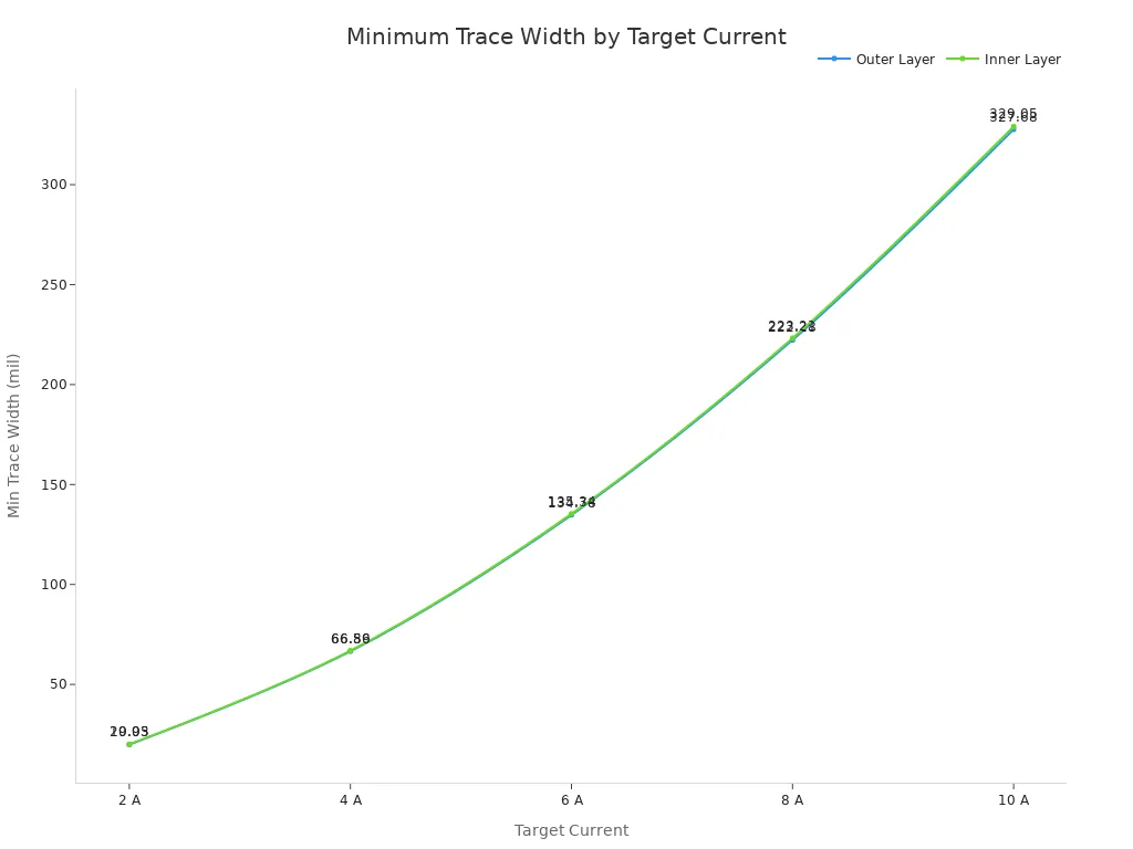
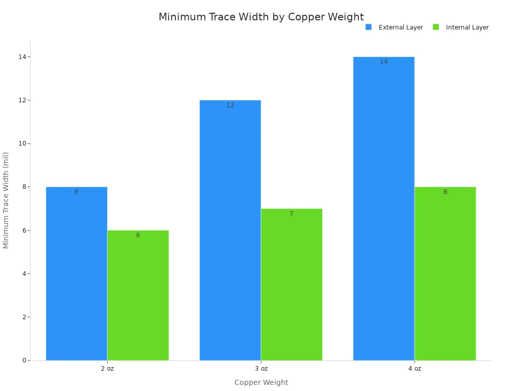
Heavy copper needs wider traces for shop etching. Change your minimum widths to match copper weights:
Copper Weight | External Layer Min Trace Width (mil) | Internal Layer Min Trace Width (mil) |
|---|---|---|
2 oz | 8 | 6 |
3 oz | 12 | 7 |
4 oz | 14 | 8 |
Keep copper features away from outer edges. Safe space protects inner layers from trace shorts:
Outer Layer Copper-to-Edge Clearance: Keep at least 7 mil space to outer edges.
Inner Layer Copper-to-Edge Clearance: Keep 10 mil space to stop stress and EMI.
Set strict rules in your dfm manufacturing process. Good design steps save thin traces during etching.
Solder Mask Webbing and Clearance
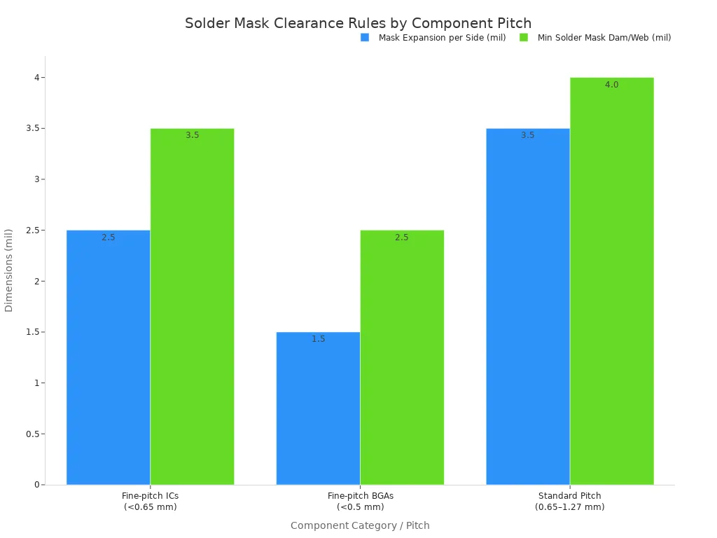
Solder mask covers copper and stops unwanted solder shorts. Mask strips between pads are called mask webs. Thin webs break easily under factory limits. Broken mask bits slide into solder, opening connections.
Standard rules ask for 0.075 mm mask webs. Factories prefer 4 mil webs to stop peeling.
Component Category / Pitch | Mask Expansion per Side | Minimum Solder Mask Dam/Web |
|---|---|---|
Fine-pitch ICs (<0.65 mm) | 2 to 3 mil | ≥3 to 4 mil |
Fine-pitch BGAs (<0.5 mm) | 1 to 2 mil | ≥2 to 3 mil |
Standard Pitch (0.65–1.27 mm) | 3 to 4 mil | ≥4 mil |
Pick correct pad styles for pin counts:
Use Non-Solder Mask Defined pads for general builds.
Use Solder Mask Defined pads for tight leads. Smaller apertures control wetting and stop bridging.
Keep traces 4 to 6 mil from mask openings.
Use gang mask openings if webs fall under 3 mil. Grouped openings remove thin dams to prevent loose bits.
Tight mask controls boost total factory output. A smart dfm manufacturing process finds clearance errors early.
Component Clearance and AOI Standards
Part layouts control assembly and soldering steps. Tight parts cause bad factory risks. Camera tools need clear views to check solder joints. Tall parts block view lines to smaller neighbors.
Defect | Soldering Process | Mechanism Caused by Improper Spacing |
|---|---|---|
Reflow Soldering | Uneven heat melts one side first, lifting the part. | |
Shadowing | Wave Soldering | Tall parts block solder flow to smaller rear connections. |
Tombstoning happens when thermal shifts melt one side fast. Surface tension then pulls the part up off pads.
Wave shadowing happens when big parts block small parts. The large body blocks solder flow, leaving open joints.
[Flow Direction of Solder Wave --->]
  +------------------+         +-----------+
  | Tall Component   |  Shadow | Small Part| <-- Starved Joint (Open)
  |                  | ======> | (Hidden)  |
  +------------------+         +-----------+
Enforce clear spacing rules across every layout:
Place two-pin parts parallel in wave lines.
Keep safe space so cameras see every joint.
Match thermal mass to balance melting speeds.
Automated checks keep production running smoothly. Use a full pcb dfm list before mass builds. A set dfm manufacturing process stops placement risks early.
Pre-Production PCB DFM Checklist
You check files before volume release. A complete dfm checklist pcb stops delays. A simple pcb dfm checklist tests strategy. A dfm manufacturing process secures parts.
BOM Lifecycle and Sourcing Accuracy
Engineers work with factory teams. Special engineers monitor part health early. They find risks before production starts. You check parts in four steps:
Perform BOM Lifecycle Audits: Check all parts in online lists.
Identify NRND Indicators: Find old parts that fade away fast.
Stock and Source Evaluation: Compare stock numbers to future needs.
Automate Risk Tracking: Set fast alerts for stock changes.
2D Drawings and CTQ Dimensions
Run a pcb dfm checklist for sizes. Follow simple rules in checklist steps:
Category | Verification Check Item | Minimum Tolerances / Guidelines | Operational Target / Recommendations |
|---|---|---|---|
Drill Specifications | Smallest Drill Size | 0.20 mm for standard mechanical drill; 0.10 mm for microvia | 0.25 mm minimum for reduced fabrication costs |
Solder Mask | Mask-Defined vs Non-Mask | Define SMD vs NSMD pad styles in fab files | Prefer NSMD for superior self-alignment and reflow area |
Silkscreen | Clearance to Pads | 5 mil minimum distance from mask openings | Automate via CAD clipping to prevent solder contamination |
Teams use a dfm checklist during layout. Check steps before final factory release:
Documentation & Files: Check all board files and netlists.
Stackup Analysis: Check layer shapes and thermal matches.
Signal & Trace Integrity: Check trace space and power limits.
Panelization Setup: Check board array shapes and marks.
Fabrication Notes and Gerber Output
Clear notes stop bad factory mix-ups. Follow a dfm manufacturing process now. Run a full pcb dfm checklist. Use a dfm manufacturing process on layers. Keep good design rules for production. A dfm checklist guarantees accurate files.
Add clear notes to stop board mistakes:
Hole Specifications: Hole sizes, limits, and metal plating.
Dimensions & Tolerances: Board shapes and hole edges.
Layer & Material Specs: Layer copper weights and board depth.
Finishes & Coatings: Surface metal, mask rules, and ink text.
Advanced Processing: Signal resistance limits and hole fills.
Communication: Phone numbers for engineering support.
Board files need clear IPC-4761 layers. The final review guards board counts. You approve files with full confidence. This last dfm checklist pcb finishes checks.
You move from late fixes to early dfm manufacturing process execution. First, build fast talk loops with suppliers. Standard DFM steps help every pcb layout, trace, pad, and layer. A strong DFM Review Process improves all builds. You use a good DFM Review Process to drop costs. Next, daily reviews save each pcb file, via, array, panel, stackup, and assembly. Also, a smart dfm manufacturing process ensures good builds. This reliable dfm manufacturing process checks key metrics:
Scrap Rate & First-Pass Yield (FPY): Cuts trash.
Cost of Poor Quality (COPQ): Cuts money loss.
Warranty Claim Rate: Makes products last long.
FAQ
What is the main goal of a dfm review process for pcb design?
Run a dfm review process. Catch pcb errors early. Save cash fast. Fix bad layout flaws. Cut pcb scrap now. Drop factory costs quickly.
When should you run a pcb dfm checklist?
Run a pcb dfm checklist early. Check CAD layout steps. Stop late board redesigns. Find small clearance issues. Help factories build pcb boards.
How does a dfm checklist pcb help hardware engineers?
A dfm checklist pcb helps daily decisions. Check drill limits fast. Review trace gaps and copper space. Stop component errors. Boost product yields easily.
Why do engineers need a generic dfm checklist before production?
A complete dfm checklist unifies design rules. Check BOM availability and Gerber layers. Stop unexpected pcb manufacturing delays. Complete checks before tool release.
What is the difference between simple testing and total dfm execution?
Simple tests spot flaws later. Early dfm simplifies pcb assembly steps. Stop shop risks quickly. Build quality pcb items without delay.
See Also
Top Surface Mount Technology Strategies For Superior Electronics Manufacturing
Essential Guidelines For Achieving Automotive Grade Surface Mount Assembly
Crucial Techniques For Mastering Dual In Line Package Electronics
Critical Reflow Soldering Standards Necessary For Surface Mount Success
Smart Ways To Optimize Your Hardware Production For Excellence
