Comprehensive Smart Home PCBA Solutions and Design Strategies
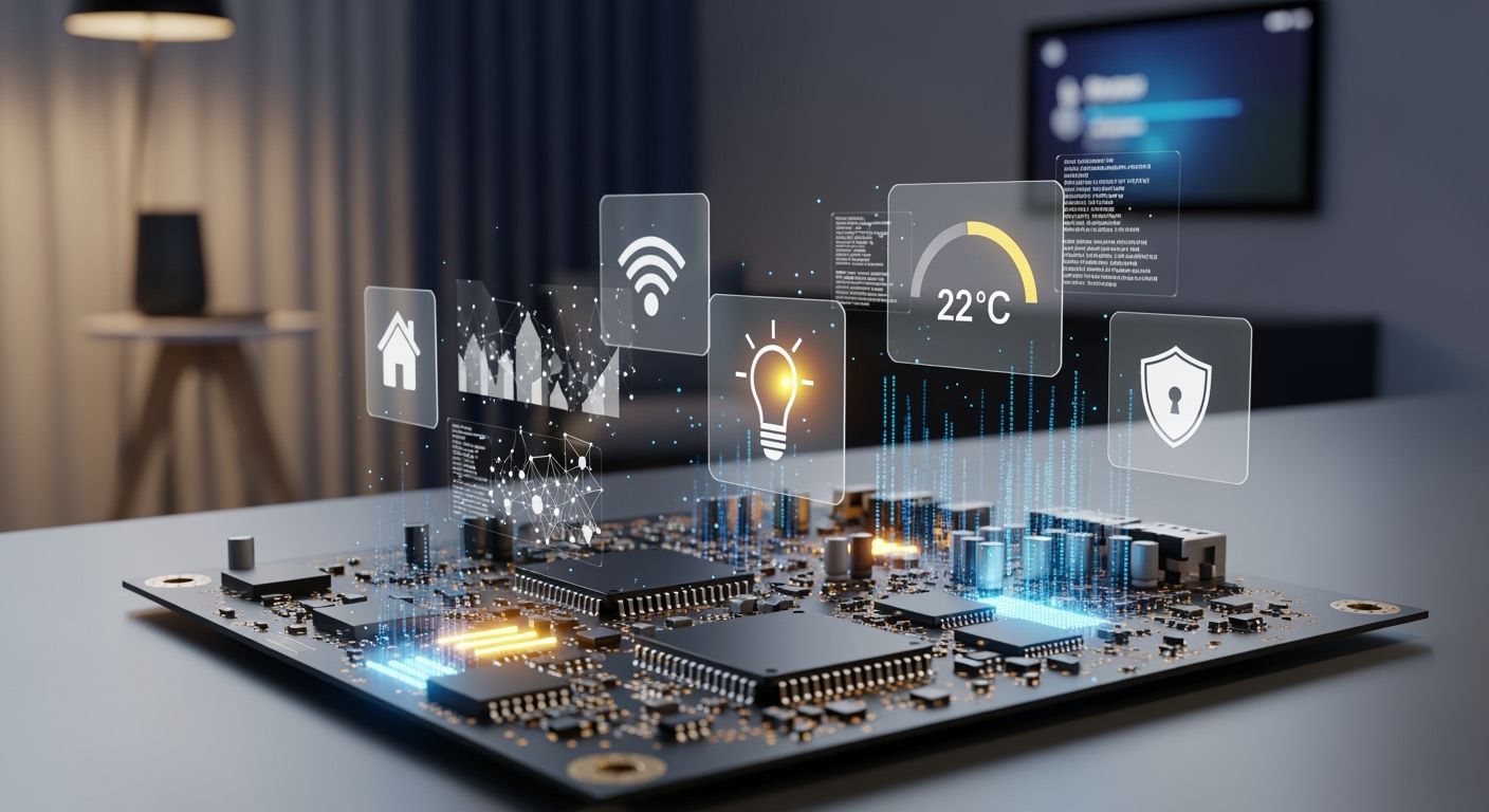
The global demand for smart home pcba modules grows steadily in the electronics market. A central smart home automation pcba reads complex sensor inputs and sends key data across an iot network. Modern automated systems need small sizes, low energy use, quick response times, and strong signal connections. Engineers choose custom smart home pcba solutions to fit tight spaces and help devices last longer. Advanced hardware parts improve how power moves through smart devices. Specialized factory partners help hardware builders by using compact circuit designs, choosing parts carefully, making good modular layout choices, and delivering reliable mass production in a busy market.
Key Takeaways
Smart home circuit boards power lighting, security systems, and climate controls efficiently.
Engineers put warm parts away from sensors so the temperature readings stay correct.
Tiny wiring methods like microvias help makers fit complex circuits into small cases.
Smart board designs help Wi-Fi, Bluetooth, and Zigbee signals stay strong without blocking each other.
Low-power sleep modes and energy gathering tools help batteries last for many years.
Factories follow strict quality rules like IPC-A-610 to build dependable smart products.
Protective coatings keep delicate electronic parts safe from dust, water, and spilled household chemicals.
Primary Smart Home PCBA Applications
Modern home designs use smart home pcba solutions to coordinate hardware tasks across connected spaces. Main processing cores read input data from smaller circuits and send commands through home networks quickly to ensure fast system responses.
Smart Lighting and Environmental Controls
Dimming Driver and Impulse Control Circuits
Engineers design every lighting control pcba to manage light levels accurately. Main power stages feed high-frequency pulse-width modulation drivers to change output brightness safely without causing visible electrical flicker. Fast switching commands require low-noise paths across the board layout. Shielded copper traces separate fast driver signals from sensitive power monitoring parts to keep signals clear over long periods of use.
Color Tuning and Ambient Sensor Interfaces
A specialized lighting control pcba checks surrounding light levels with a dedicated optical sensor interface. Microcontrollers figure out exact color settings to change light tones smoothly inside modern home rooms. Small board designs place sensitive sensor inputs far away from hot driver parts. This smart physical separation keeps the system stable and accurate during continuous daily use.
Security Systems and Access Control Boards
Video Streaming and Camera Interfaces
A high-speed security system pcba handles live video feeds from high-definition camera units. Special signal traces carry raw video data directly to powerful digital processing chips without losing any information. Data compression parts reduce sending delays over local wireless networks. Careful board wiring protects high-frequency communication channels from digital noise to keep video feeds clear on extra devices.
Smart Lock Actuator and Biometric Controls
Another security system pcba controls motor drivers and biometric verification parts. Physical access control hardware checks user details right away to protect home entrances against unwanted visitors. Battery protection circuits shield the home automation pcba from harmful voltage drops during heavy motor use. Low-power standby modes help the battery last for several years of steady service.
Climate Automation and Energy Monitoring
HVAC Relays and Thermostat Controllers
Modern smart home automation systems need strong relay driver circuits. Solid-state switches turn on heavy HVAC blowers and heating compressors without mechanical wear or physical damage over time. Direct communication paths connect local relays with central smart devices. Smooth system setup keeps indoor temperatures steady across different living areas through every season of the year.
Current Sensing and Power Metering Circuits
Engineers build board layouts for smart home energy monitoring with special current transformers. Accurate shunt resistors measure large electrical loads across active home appliances at all times. Advanced smart home pcba solutions send accurate diagnostic data to external smart devices. These smart units reduce electrical power use across the entire network easily.
Core Design Strategies for Smart Home Hardware
Multi-Sensor Integration and Processing
Temperature and Humidity Sensor Layouts
Engineers position heat-generating parts with great care on tiny circuit boards. Special cutout gaps isolate warm power converters from delicate temperature-sensing chips on the pcba surface.
Copper layers draw extra heat away toward the outer edges of the board. This smart physical separation boosts measurement accuracy while sensors collect data continuously for modern home devices.
Motion Detection and Noise Isolation
Motion detection parts work with weak analog signals from light and radar tools. High-frequency digital noise easily disrupts these delicate signal lines if solid copper shielding is missing.
Engineers place sensitive analog paths on middle board layers between solid ground shields. This smart layout protects clear signals while helping designers add more sensor features to devices.
High-Density Interconnect and Miniaturization
Microvia Applications in Compact PCBAs
Engineers use high-density wiring methods to create tiny smart home pcba designs. Microvias link thin copper layers inside tight board spaces without taking up valuable surface area.
HDI process tier | Minimum trace width | Minimum spacing | Manufacturing note |
|---|---|---|---|
Standard HDI | 50–75 μm | 50–100 μm | Common baseline for reliable fabrication |
Advanced HDI | 25 μm | Matching or slightly larger than trace width | Requires precise etching and advanced processes |
Fine-line capability | 25–50 μm | Not separately specified | More complex and costly to fabricate |
Some manufacturers' reliable limit | 75 μm | Not separately specified | Achievable without additional cost |
Advanced factory methods reach a thin 25 μm trace width for tightly packed wiring layouts. Standard HDI methods use 50–75 μm trace widths with 50–100 μm spacing to ensure reliable board building.
Rigid-Flex Substrate Selection Techniques
Rigid-flex boards join flexible plastic strips with sturdy FR-4 multi-layer sections. Designers bend these flex parts into tiny curved covers to remove bulky wire connectors from small pcba cases.
Moving flex sections absorb continuous mechanical stress inside active door hinges and smart gear. Designers keep copper thickness even across bend areas to help the main control board last longer.
Emerging Substrates and Fabrication Trends
Embedded Passive Components and 3D Electronics
Makers hide passive parts directly inside core board layers while stacking the materials. Internal placing frees up outer space for larger main processor chips and main communication paths.
3D printed bases let engineers run circuit lines along custom curved shapes. This new building style helps modern smart home tech fit into unique product covers across a growing industry.
Biodegradable Substrates for Eco-Friendly IoT
Green manufacturing methods push board research forward across global tech markets. Makers test plant cellulose and dissolving polymers to replace regular glass-epoxy bases in basic iot devices.
These eco-friendly materials break down safely in natural waste streams after disposal. Sustainable smart home pcba options help spread iot technology around the world without making extra electronic trash. Modern devices use these green methods to keep home control systems running cleanly.
Wireless Connectivity in IoT Smart Home Systems
Multi-Protocol Hardware Integration
Coexistence for Wi-Fi, BLE, and Zigbee
Engineers put several radio parts on the main circuit board surface. These radios can disrupt each other while sending wireless signals. Time-division sharing lets radios use the antenna path safely together. High-pass filters block bad signal noise near sensitive receiver circuits.
Placing radio chips farther apart stops signals from overlapping. Ground cutouts lower extra radio energy near high-frequency board paths. Designers set up clear data priority rules to stop connection drops in control systems.
Matter Standard Hardware Requirements
The Matter system connects different smart brand tools across home networks. Modern control chips need larger memory spaces to run complex security codes. Designers pick processing chips with special built-in safety tools to guard network keys.
Using connected iot tech simplifies initial setup for basic smart tools on varied systems. Secure startup features block fake software changes during system updates. This solid hardware base guarantees reliable wireless operation for modern home tech.
RF Layout and Antenna Placement
Trace Antenna vs Ceramic Chip Options
Engineers pick printed circuit antennas or tiny ceramic chips based on open room. Printed options cost less but need more outer board space. Ceramic chips save helpful room inside tight device cases.
Industry benchmark | Return loss / VSWR value | Interpretation |
|---|---|---|
Robust commercial product | VSWR < 2.0, equivalent to return loss < -9.5 dB | Approximately 90% of power is delivered to the antenna structure |
General PCB antenna design | 10 dB return loss | 90% of incident power reaches the antenna for radiation; 10% is reflected |
Impedance Matching and Ground Planes
A matching circuit tunes board signal lines to fifty ohms impedance. Good tuning stops signals from bouncing back between sender and antenna parts. Engineers keep bottom ground layers solid under fast signal lines.
Unbroken ground layers give smooth paths for high-frequency electric streams. Small board holes along ground edges lower extra radiation from line borders. This careful layout keeps signal strength strong for smart home tools.
EMC and Board Shielding Techniques
Shielding Can Placement for Receivers
Metal shield covers block outside electrical noise from reaching delicate radio receivers. Designers solder ground frames right over main processor chips and radio parts. Solder points around the frame edge make solid contact with ground layers.
Pop-off metal tops let workers check parts quickly during quality tests. Placing frames right keeps receivers working well near noisy power paths. This extra protection helps the main system run well in busy homes.
Parasitic Capacitance Suppression
Unwanted electric capacitance messes up high-speed signals along thin copper lines. Designers widen line spacing to stop bad power jumps between nearby paths. Clearing ground copper under antenna pads boosts wireless output.
Placing extra small parts carefully lowers signal issues on high-speed lines. Short trace lines reduce total power loss across the smart circuit board. Better circuit shapes keep radio links steady across all working devices.
Power Management and Energy Efficiency
Efficient power management reduces electricity costs across residential environments. Engineers design intelligent circuits to regulate current flow throughout each board. Proper power distribution improves overall system reliability.
Low-Power States and Energy Harvesting
Microcontroller Deep-Sleep Mode Routing
Engineers place dedicated copper traces to wake up dormant processing units quickly. Power switches isolate inactive peripheral zones during low-activity periods. This routing strategy drops total power consumption significantly.
Fast signal lines handle critical interrupts without activating main system clocks. Small board layout loops prevent leakage current from draining backup power reserves. Smart power routing maintains precise control over sleep cycles.
Ambient Light and Thermal Harvesting
Tiny solar cells gather energy from ambient indoor lights. Photovoltaic collectors convert room light into low-voltage direct current. Thermoelectric generators convert heat differences into usable electricity for smart devices.
Specialized components boost weak energy signals to stable operating levels. This continuous supply powers secondary sensor nodes without extra wires. Energy harvesting improves energy efficiency across modern home networks.
Battery-Powered System Optimization
Lithium-Ion Charging and Protection
Integrated circuits monitor battery cells during operational cycles. Dedicated protection networks disconnect power paths during overvoltage or short-circuit events. Specialized temperature sensors stop charging procedures under hot ambient conditions.
Effective copper heat sinks keep power conversion components cool on the main board. Safe charging routines prolong battery operational life.
Fuel Gauge IC and Voltage Regulation
A fuel gauge IC tracks remaining capacity by monitoring current flow. Small shunt resistors measure electrical draws accurately. Low-dropout regulators deliver steady voltage levels to sensitive processing chips.
Efficient switching regulators optimize power conversion for active wireless radios. Stable voltage control prevents random system resets during heavy transmission periods.
Mains AC-DC Power Converter Design
Flyback Switching Power Integration
Flyback converters change high-voltage alternating current into safe low-voltage direct current. Isolated transformers physically separate high-voltage lines from secondary low-voltage circuits. Modern power controllers reduce standby power losses during idle states.
Compact inductors filter switching noise off the main pcba board. Sound power topology maintains high conversion efficiency across smart home systems. Seamless integration of power stages reduces board space requirements.
Transient Suppression and Surge Protection
Metal oxide varistors absorb high-voltage transients from municipal electrical grids. Transient voltage suppression diodes clip sudden voltage spikes before sensitive pcba components receive damage.
A smart home pcba must meet strict safety standards for residential installations. IEC 61000-4-5 testing defines specific surge protection levels based on the installation setting:
Installation setting | Standard class | Surge withstand voltage |
|---|---|---|
Residential/commercial (smart-home mains PCBA) | Class 2 | 1 kV |
Proper clearance distances prevent electrical arcing across high-voltage traces. This protective hardware keeps smart home automation devices running safely over long operational lifespans.
EMS Selection for Smart Home PCBA Solutions
Selecting an experienced electronics manufacturing services partner ensures reliable device creation. The global demand for smart home pcba modules forces companies to select factories with precise technical capabilities. Superior factory execution turns complex hardware blueprints into stable final products.
Technical Capabilities and ISO Standards
Precision Surface Mount Technology
Modern automated placement lines handle micro-sized passive parts and dense integrated chips. Advanced robotic pick-and-place equipment places tiny parts on small copper pads with extreme accuracy. Reflow ovens maintain strict thermal profiles to melt solder paste evenly across all circuit board layers.
Precision equipment prevents common soldering defects during fast production runs. Specialized optical sensors verify exact component alignment before boards enter high-temperature heating zones. High placement accuracy protects delicate electrical channels across dense circuit boards.
ISO9001 and IPC-A-610 Compliance
Quality certification standards guide reliable board assembly. Electronics factories follow ISO9001 rules to track quality control across every assembly step. Production teams use IPC-A-610 visual standards to judge solder joints accurately.
Selecting the proper IPC acceptance class protects product budgets and field performance.
Class 2 standard: Serves as the default standard for dedicated smart home appliances in normal indoor environments.
Class 3 standard: Covers critical systems where operational failure causes severe hazard or catastrophic system loss.
Trade-off strategy: Over-specifying Class 3 when Class 2 works raises product costs through slower inspections and excess rework.
Class | Smart-home PCBA applicability | Reliability and failure impact | Examples from source |
|---|---|---|---|
Class 2 - Dedicated service | Default for standard smart home appliances | Extended reliable service in normal environments; failure is undesirable but not catastrophic | Smart home appliances, industrial equipment, EV charging systems |
Class 3 - High-reliability electronics | Required for safety-critical or mission-critical smart home functions | Very long life and mission-critical reliability; failure could cause serious injury, mission failure, or system-level catastrophe | Medical life-support, aerospace, defence, safety-critical automotive and e-mobility systems |
DFM and Testing Protocols
Automated Optical and In-Circuit Testing
Automated optical inspection units scan finished circuit assemblies using high-resolution camera tools. Visual algorithms catch missing parts, misaligned pins, and bad solder bridges right away. In-circuit testing probes confirm proper electrical values across every circuit path.
Functional testing rigs power up assembled boards to check wireless responses. Automated test sequences send test data packets to verify active radio performance. Thorough testing steps filter out broken parts before final delivery.
Early DFM Reviews for EOL Mitigation
Design for manufacturability reviews identify layout issues before factory production starts. Engineers check component clearance rules to speed up automated assembly steps. Early feedback prevents expensive circuit board revisions during later manufacturing phases.
Engineers track component lifecycle status to spot end-of-life risks early. Swapping obsolete parts during early design stages prevents sudden supply stops. Proactive component tracking keeps factory assembly moving smoothly.
Turnkey Supply Chain and Box-Build Assembly
Component Sourcing and Traceability
Turnkey manufacturing partners handle global procurement channels to source genuine silicon parts. Trusted supply networks stop fake components from entering factory assembly lines. Automated tracking systems store unique batch numbers for every component reel.
The seamless integration of iot technologies depends on predictable component deliveries. Traceability databases record production dates and supplier details for every board. Clear part records help factories resolve quality issues quickly.
Enclosure Assembly and Conformal Coating
Box-build services combine finished boards with external plastic cases and wiring harnesses. Factory technicians install protective silicone seals to block moisture from entering final consumer products. Complete assembly services reduce total transit costs for product owners.
Protective conformal coatings shield raw circuit traces against high humidity, dust, and domestic chemical spills.
Applying thin protective layers extends operational life inside harsh home environments. Complete turnkey smart home pcba solutions deliver tested products directly to retail distributors. Hardware creators gain strong market advantages by using complete smart home services. Specialized manufacturing solutions allow companies to launch reliable smart home pcba designs in a competitive market.
Strong circuit design directly controls performance, energy savings, and working lifetime across all connected systems. Growing global demand for smart home PCBA modules forces companies to use modern hardware trends. Engineers build reliable smart devices by using modular layouts and advanced factory methods. A well-designed home automation PCBA lowers long-term repair costs and improves network stability in a fast-moving market. Custom smart home PCBA solutions boost overall product performance for competing brands. Hardware makers should pair up with skilled EMS providers to secure full manufacturing support and speed up market success. Expert production partners provide scalable solutions that turn initial ideas into high-performing commercial products.
FAQ
Which standards fit smart home PCBA solutions?
Factory lines follow IPC-A-610 Class 2 rules for normal home gear. This benchmark ensures steady performance in regular houses without raising production expenses needlessly.
How do designers shrink modern IoT gear?
Engineers pick high-density wiring methods like microvias to clear surface space. Modern factory steps trim copper line widths down to 25 μm. These tight layouts allow smaller product builds for everyday users.
How do multi-protocol circuits block signal interference?
Smart layouts spread radio chips apart and clear out ground copper to stop crossing signals. Designers also use shared time slots. These hardware tweaks keep wireless links steady across all active systems.
Why do hardware teams need custom home automation boards?
Tailored layouts boost energy use and fit inside small plastic covers. Custom designs speed up sensor paths while making products last longer in a busy market.
How do low-power states help connected devices?
Chips use special wake-up paths to shut down idle areas during quiet times. This wiring trick stops extra battery drain. As a result, battery-powered gear runs safely for several years.
How does conformal coating guard main control boards?
Workers spray thin coating layers across bare circuit lines. This outer shield guards delicate parts against household chemical spills, dirt, and wet air. Good protection keeps devices running well over long periods.
What materials support greener technology choices?
Makers test plant fibers and melting plastics instead of standard glass-epoxy bases. These eco-friendly base options decay safely in natural garbage sites after disposal.
See Also
Understanding Essential Printed Circuit Board Assembly Concepts And Components
All Inclusive PCBA Solutions Covering Fabrication Through Final Testing
Navigating Complete Circuit Board Assembly Processes From Production To Inspection
Maximizing Your Enterprise Productivity With Turnkey Electronics Contract Manufacturing
Decoding Printed Circuit Board Assembly Terminology In Modern Electronics
