WiFi Module Integration in PCBA Design

You achieve successful wifi module integration by following strict pcb layout design rules. You must keep a 50 Ω characteristic impedance on RF traces. Board factories offer ±10% variation for RF lines on four-layer boards. You protect signal strength when your RF trace gets a return loss of S11 ≤ -10 dB and a VSWR ≤ 2:1.
Proper wi-fi module location guards your signal path. You must place main ground layers under wifi traces. Smart antenna choice and placement stops wi-fi signal loss. Remove all copper from antenna keepout zones. Steady power lines supply clean wifi energy during data sending. These steps boost board layout quality for pcba design and wireless tech on your pcb.
Key Takeaways
Ready-to-use Wi-Fi modules save time and lower testing expenses when making products.
Keep RF traces at 50 ohms impedance to get a strong wireless signal.
Remove all copper and metal from the antenna areas to keep the signal strong.
Put capacitors close to power pins so the voltage stays steady while sending data.
WiFi Module Integration vs. Chip-Down Options
Making custom RF circuits needs special testing tools and skilled engineering teams. Picking pre-certified units simplifies your overall pcba design. You speed up project work and lower money risks during production.
Selecting Pre-Certified Wi-Fi Module Options
Pre-certified Wi-Fi modules let engineers add wireless connectivity without building Wi-Fi from scratch and avoid the lengthy, costly end-device regulatory approval process, significantly reducing development time and time-to-market.
You make hardware design easier by placing a pre-certified wi-fi module on your board. Custom designs cost $18k–$58k+ in testing and engineering fees. Pre-certified choices drop total testing costs to $3k–$8k while shortening development from 8–16 weeks to 2–6 weeks. A pre-certified wi-fi module includes FCC, CE RED, or IC approvals. These approvals protect your wireless technologies during production.
Custom RF design | Pre-certified module |
|---|---|
$18k–$58k+ total estimate | $3k–$8k plus module cost |
8–16 weeks timeline | 2–6 weeks timeline |
Choosing the right wi-fi module means checking heat limits and data speeds. You need a 4-layer board with 50 Ω RF traces for dual-band wireless technologies. Make sure your power supply gives 1.2 A of current to stop heat slowdowns. Wise module choices raise wifi pcb manufacturing output. They also cut signal noise in wireless communication devices inside factory spaces.
Interoperability with Host Processors
You join the wi-fi module straight to an ARM-based host controller for fast data movement. The host system handles wireless network traffic using software drivers. Hardware connections like UART, SPI, or SDIO make stable links between chips. SDIO links handle clock speeds up to 25 MHz in full-speed mode. These digital paths keep clean signals across your pcb layout design.
Matching signal voltage levels stops communication errors on the board. The GPIO and SDIO I/O power line works from 1.71 V to 3.63 V. You have to match the main driver voltage to the module interface line. Correct power settings stop data mistakes during fast wifi transfers. Smart layout choices ensure smooth wifi module integration for your project. Careful pcb routing keeps wifi working steadily during wifi pcb assembly. You get strong wifi performance using proven pcb layout design methods for wireless technologies. Good layout steps make wifi pcb manufacturing simple while improving your pcba build. Using a certified wi-fi module guarantees easy setup for modern wireless technologies.
PCB Stackup and WiFi Layout Principles
You safeguard wireless signals by selecting a solid stackup in your pcba design. Placing a unbroken ground reference right under traces creates low-resistance return paths. Smart ground plane placement stops radiation loops, protecting trace paths from unwanted noise. Clean routing ensures smooth high-speed data flow across your board layout.
Ground-plane feature | EMI reduction | Signal-integrity preservation |
|---|---|---|
Return current beneath trace | Minimizes loop area | Reduces noise distortion |
Continuous copper plane | Blocks external fields | Shields wireless signals |
Dedicated Ground Planes and Interference Control
You stop signal loss by adding ground via fences along both sides of the RF trace. Keep stitching-via spacing under λ/20 based on the working frequency. Space these vias 6 mm or less for 2.4 GHz, and 3 mm or less for 5 GHz mode.
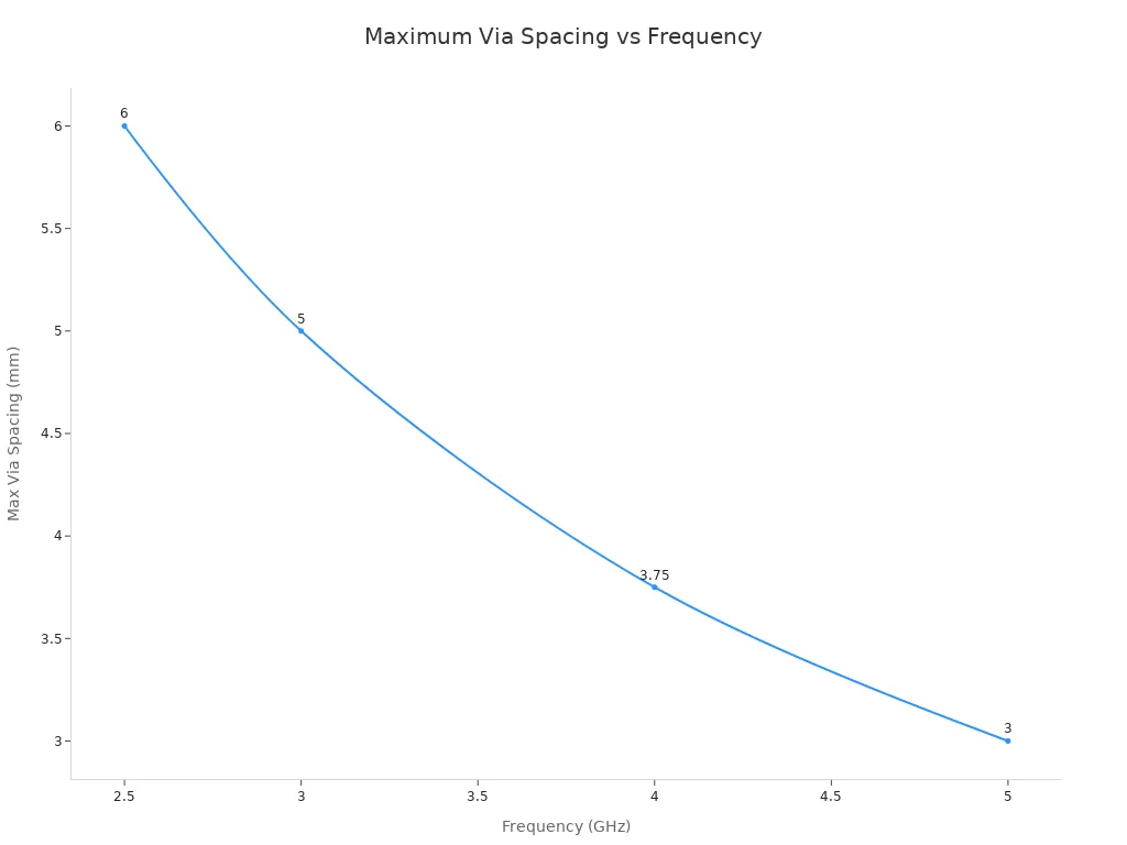
Solid ground reference planes protect signal health for all wireless technologies. An uninterrupted reference plane holds your target trace impedance across the full wi-fi layout. Execute pcb layout design carefully. Run signal testing early in your pcb layout design phase to check noise control before starting wifi pcb manufacturing.
Characteristic Impedance Control Methods
You get exact 50-ohm trace control by setting layer stackup sizes inside your pcb layout design. Standard four-layer FR4 boards use a total thickness of 1.57 mm (62 mil) with a ~42 mil core and 7 mil prepreg layers. Route 50-ohm single-ended RF lines using 13 mil width plus 26 mil clearance.
Parameter | Value |
|---|---|
Board thickness | 1.57 mm (62 mil) |
Core thickness | ~42 mil |
Prepreg Dk for FR4 | 4.1 |
Trace width | 13 mil |
Copper clearance | 26 mil |
You ease wi-fi module integration by matching parts in your pcb layout design. An 8.17 mil (0.208 mm) prepreg dielectric with Dk of 4.3 and 1.8 mil copper using 13.2 mil (0.335 mm) trace width yields 50.6 Ω impedance. Picking a good wi-fi module and adjusting your pcb layout design keeps wifi signal quality steady. Every wi-fi module depends on set impedance during daily wifi operation. Proper wifi routing stabilizes your connection during wifi pcb manufacturing. Strict layout habits boost wifi performance through wifi pcb manufacturing, securing wireless technologies for your main wifi device.
Antenna Placement and RF Isolation Rules
Clever choice and setup of antennas keeps your wireless path safe on the board. Put your wi-fi module close to corners for best energy output. Do not place metal items like batteries or screws right above the antenna. Such items ruin radiation shapes, detune antennas, and cause trace mismatch.
Bad metallic coatings stop radio waves and hurt overall power output. This signal drop ruins link quality by 10–30 dB. You stop weak wireless connections by keeping the antenna zone empty.
Proximity condition | Effect on radiation efficiency | Effect on return loss / link budget |
|---|---|---|
Insufficient clearance around walls, shields, or screws | Detunes antenna, lowers efficiency, shrinks range | Increases reflected power and lowers receiver RSSI |
Conductive decorative finishes near the module | Distorts radiated fields and reduces net gain | Increases mismatch losses, lowering link margin by 10–30 dB |
Keepout Zones for Patch Antenna Layouts
Keep clean keepout zones on every board layer below the patch antenna. Do not run power lines, digital signals, or copper fills inside this saved space. Ground cutouts prevent extra capacitance from dragging the antenna off its main frequency. Clear areas keep signals strong during active data transfer.
Good wifi antenna placement needs open space around the sending part. You protect soft wireless tech from board noise by keeping strict clearances. Wise pcb layout design stops ground loops from cutting down wifi strength. Good layout plans ensure steady wireless links for all user gear.
Shielding and Trace Clearance Techniques
Separate fast wifi traces from noisy clock lines using grounded guard traces. Setting smooth ground layers around inner RF lines creates a clear return path. Running grounded rings next to sensitive wireless parts blocks unwanted board noise. These layout walls block signal noise across your whole pcb design.
+----------------------------------------------------+
|  [ Shield Trace ] - - - Grounded Line - - - - - -  |
|  ================= Wi-Fi RF Trace ===============  |
|  [ Shield Trace ] - - - Grounded Line - - - - - -  |
+----------------------------------------------------+
Stitching vias along shield edges join different ground zones across all layers. Always route RF lines away from ground gaps to prevent signal leaks. Precise pcb layout design keeps wifi paths clean during heavy work. Smart wifi module integration relies on neat pcb layout design habits. Safe layout isolation shields your final wifi device during fast work.
Power Integrity and EMI/EMC Compliance
You maintain power integrity by supplying stable current during heavy radio usage. Peak current needs depend directly on the transmit power consumption of your system. Most wireless modules send data close to full power during normal activity. Devices using 802.11n standards usually draw tens to hundreds of milliamps during active radio modes. Steady supply lines prevent sudden voltage drops during heavy wireless transmissions.
Decoupling Networks for Wi-Fi Performance
You protect wi-fi signal integrity by building a strong decoupling network on your pcb. Put a local 0.01 µF to 0.1 µF ceramic capacitor right next to the VDD pin on the same layer. Position small 0402 ceramic parts near power pins to absorb high-speed noise. Place a 4.7 µF to 10 µF bulk capacitor near power inputs to handle low-frequency load changes.
Capacitor value | Typical self-resonant frequency | Best for filtering |
|---|---|---|
10 µF | ~0.3 MHz | Low-speed voltage dips and startup transients |
1 µF | ~3 MHz | Low-frequency switching noise |
0.1 µF | ~30 MHz | Medium-speed digital noise |
0.01 µF | ~200 MHz | High-speed edge spikes and EMI |
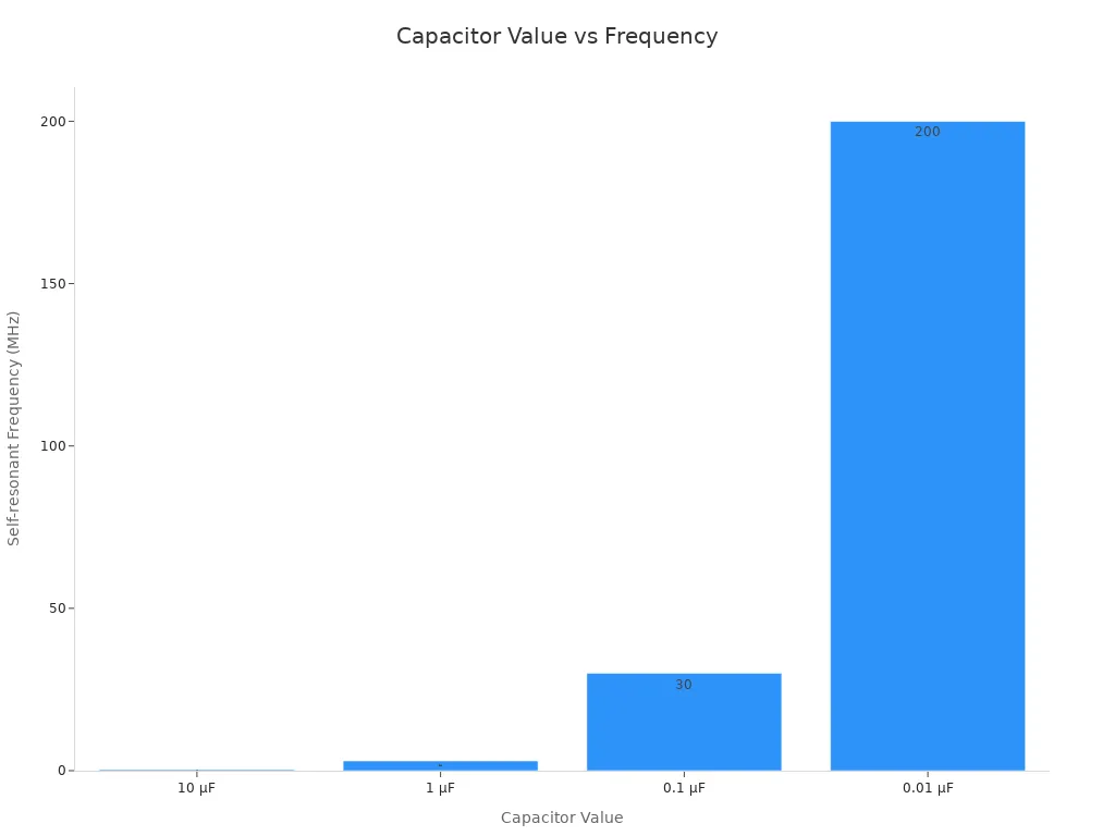
You shrink high-frequency current paths by placing vias right beside capacitor pads. Pair power and ground vias closely to lower unwanted loop inductance. Wise power routing protects sensitive wi-fi lines from noise during board building. Careful pcb layout design steps protect your overall board layout from deep voltage drops.
Thermal Vias and Suppression Methods
You cut heat accumulation by placing thermal vias right under the module ground pad. Continuous sending modes create heat that lowers radio output over time. Drill a tight 5×5 array of 0.3 mm vias spaced 1.0–1.2 mm apart directly beneath the thermal pad. A 5×5 thermal via grid drops thermal resistance by roughly 60%.
Join these thermal vias directly to large inner ground layers to spread heat across the board. Smart part placement stops hot spots from harming nearby components on your board. Careful layout choices simplify board manufacturing while raising product reliability. Following these layout steps ensures smooth board production for high-speed wireless gear.
You finish successful wifi module integration by conducting complete hardware validation. First, verify trace impedance testing, check power rail integrity under peak current, and perform thermal profiling. Signal integrity analysis helps you catch hidden noise issues early in your pcba design process.
Run this pre-tapeout checklist before starting your final wi-fi pcb manufacturing run:
Confirm continuous ground plane layers below all wi-fi RF paths.
Verify proper clearance and placement around the antenna feed.
Place every decoupling capacitor close to its matching pin on the pcb.
Disciplined layout habits secure strong wi-fi module performance. Following clean pcb layout design rules cuts expensive pcba board revisions and speeds up wireless device approval.
FAQ
How does a wi-fi module simplify wifi pcb manufacturing?
A certified wi-fi module has FCC, CE RED, and IC approvals already set. You dodge high testing fees and save engineering time. Placing a pre-certified wi-fi module makes wifi board making easier, fixes wifi signal paths, and ensures success while doing wifi pcb manufacturing.
What trace impedance rules apply to a wifi board?
You need a 50-ohm characteristic impedance on all wifi RF traces. PCB factories give exact tolerances on multi-layer boards. Good pcb layout steps protect wi-fi signal quality, keep wifi power steady, block wifi noise, and stop wifi performance drops during wifi pcb assembly.
Why do you need strict antenna keepout rules for wifi designs?
You have to clear away all copper layers under the wifi antenna. Metal items ruin wifi radiation fields and trigger a wifi impedance mismatch. Empty antenna keepout zones keep wi-fi range far, aid stable wireless connections, and shield smart wireless technologies from wifi board noise.
How do you perform final validation on your wireless board?
You check trace impedance, test wifi signal levels, inspect wifi power stability, and track heat dissipation. Full hardware checks verify that the ground plane stays complete. Using good layout habits guarantees simple wifi module integration and speeds up official approvals for new wireless technologies.
See Also
Understanding PCBA Basics And Its Essential Circuit Board Components
Sourcing High Quality Electronic Components For Successful Circuit Manufacturing
Uncovering What PCBA Truly Means In Modern Electronic Manufacturing
Combining Surface Mount And Through Hole Techniques For Better Circuitry
Choosing The Right Circuit Board Manufacturer For Your Business Goals
