Via Types in PCBA: Through-Hole, Blind, Buried
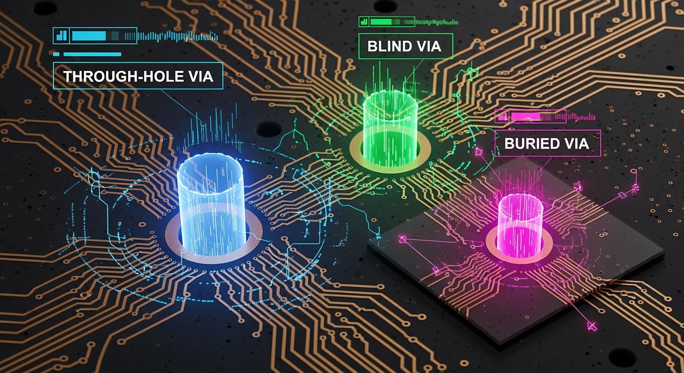
You see three main via types in PCBA: through-hole, blind via, and buried via. Through-hole vias connect every layer of a printed circuit board. Blind vias connect the outside layers to the inside layers. Buried vias only join inside layers and are not seen on the surface.
It is important to know about these vias because:
Each type has a special job in how devices work.
Picking the right one helps the device work better and be stronger.
Choosing the best vias makes building easier and saves money.
Key Takeaways
Learn about three main via types: through-hole, blind, and buried. Each type has its own job in PCB design.
Pick the right via to make devices work better and last longer. Choosing well can save money and help things work well.
Through-hole vias cost less and make strong links. They are good for simple designs.
Blind vias use less space and help signals stay clear. They are great for crowded designs like smartphones.
Buried vias keep the surface neat and let wires go many ways. They are best for advanced electronics with lots of layers.
Through-Hole Vias
Structure and Function
Through-hole vias are in almost every printed circuit board. These small holes connect all the layers together. A through-hole via starts with two pads on different copper layers. You drill a hole through the board and cover it with copper. This makes a barrel that connects the pads. Electricity can move between layers through this barrel. The barrel is shaped like a tube. Sometimes, it can break because it is long and thin. Through-hole vias connect traces from the top layer to inside layers. You can use this way for single-layer or multi-layer boards.
Advantages and Drawbacks
Through-hole vias have many good points. They make strong connections, so parts stay in place when the board shakes or moves a lot. They also give steady electrical links, so the board works well for a long time. Through-hole vias are cheap to make because the process is simple. You can use them to help with heat in high-power devices. But there are some problems too. Through-hole vias can cause signal issues because the barrel changes how electricity moves. If you do not drill or cover them right, mistakes can happen. Over time, heat can make the copper crack, and this can cause the board to fail.
Advantage | Description |
|---|---|
Cost-effectiveness | Easy to make, so they do not cost much. |
Mechanical strength | Makes a strong connection, good for stressed parts. |
Reliability | Gives steady electrical links, so fewer failures happen. |
Common Uses
Through-hole vias are used in many electronics. Power distribution uses big vias near high-power parts and small ones for other needs. EMI-sensitive circuits use ground vias to keep signals safe. Thermal management uses thermal vias to move heat away from hot spots. You also see through-hole vias near capacitors, where they connect to power and ground planes. Designers use via fences to keep analog and digital sections apart. Through-hole vias are the most common choice for routing signals and putting parts on the board.
Blind Via Technology
Blind Via Structure
A blind via is a hole you see on a printed circuit board. It connects an outside layer to one or more inside layers. The blind via does not go all the way through the board. One end is on the outside, and the other end stops inside. Blind vias help connect outside layers to inside power planes. This makes less mess and gives more space for small parts. Blind vias are very important in high-density designs. They let you add signals without making the board bigger.
Blind vias join one outside layer to one or more inside layers.
The name "blind" means one end is seen and the other is hidden.
Blind vias help link outside layers to inside planes, so you have more room for parts.
Benefits and Limitations
Blind via technology has many good points for small PCB designs. You save space because the blind via only goes as deep as needed. This leaves other layers open. The board can be 20-30% smaller. Smaller boards use less material, so you spend less money. Blind vias make signals better by making the path shorter. This helps stop signal bounce and crosstalk. You also do not get stubs that can mess up signals. Blind vias give you more ways to add traces and parts. You can fit more things on each layer and make the circuit denser.
Limitation Type | Description |
|---|---|
Depth-to-Diameter Ratio | Blind vias should not be deeper than ten times their width. |
Manufacturing Complexity | Blind vias need careful work, which can cost more. |
The smallest blind via is about 0.15 mm to 0.2 mm wide.
Keep the blind via aspect ratio at 10:1 or less for best results.
Make sure blind vias and pads are spaced right to stop signal problems.
Try not to use via-in-pad unless you must, because it can cause trouble when making the board.
Applications in High-Density PCBs
Blind via technology is used in high-density interconnect PCBs. It connects certain layers without touching others. Blind vias save space and can make the board 20-30% smaller. In boards with many layers, blind vias let you add up to 50% more traces inside than through-hole vias. Blind via technology lets you put more parts and traces in a small space. You get more options and can make small, strong devices.
Tip: Blind via technology is very important for smartphones, tablets, and other devices where space is tight.
Buried Via Applications
Buried Via Definition
A buried via connects only the inside layers of a printed circuit board. It does not go to the top or bottom surface. You cannot see a buried via from outside the board. It stays hidden inside, so the board looks neat. This makes the board look clean and tidy. Here is a table to compare buried vias with other types:
Via Type | Definition | Visibility |
|---|---|---|
Buried Vias | Connect only inner layers and are not visible from the outside. | Not visible from outside |
Through-Hole | Extend from the top to the bottom layer and are visible on both surfaces. | Visible on both surfaces |
Blind Vias | Connect an outer layer to one or more inner layers, visible from one side. | Visible from one side |
A buried via lets you link signals between inside layers. You do not need to use the surface for these connections. This makes it easier to plan the board. The outside layers stay open for other parts.
Pros and Cons
Buried vias have many good points for PCB designs. You can make the board smaller and fit more circuits inside. The outside layers stay open for important parts or traces. Buried vias help lower crosstalk and signal noise. This keeps your signals strong and clear. You can use buried vias to make complex boards with many layers. These boards work well in small devices.
Advantage | Description |
|---|---|
Keeps outer layers clean | Buried vias do not appear on the board surface, allowing for critical routing or component placement. |
Supports high layer counts | Essential for multi-layer HDI PCBs where multiple internal planes must interconnect. |
Improves signal integrity | Isolating signals inside the PCB stack reduces interference from outer-layer routing. |
There are some problems too. Buried vias are hard to make. You need special tools to drill and cover them with metal. This can cost more money. If something goes wrong, you cannot see the buried via from outside. This makes fixing problems harder.
Disadvantage/Challenge | Description |
|---|---|
Manufacturing difficulty | Requires precise drilling and plating, increasing cost and complexity. |
Accessibility issues | Difficult to troubleshoot and repair due to invisibility from the surface. |
Aspect ratio considerations | Larger ratios complicate manufacturing and may raise costs. |
Use Cases in PCB Design
Buried vias are used in many advanced electronics. You see them in high-density PCBs, industrial controls, and aerospace systems. Buried vias help you build complex boards with many layers. You can route signals inside the board and keep the surface open for chips and connectors. This makes your design flexible and strong. Buried vias also let you use fewer routing layers. This can save space and lower costs. You use buried vias when you need high performance and small size. They are common in smartphones, tablets, and other smart devices.
Tip: Use buried vias when you want to fit more circuits without making the board bigger.
Vias Comparison and Selection
Key Differences
There are different vias in PCB design. Each via type has its own job. Through-hole vias go through the whole PCB. Blind vias link the outside layer to inside layers. Buried vias stay inside and never reach the surface. Here is a table to compare them:
Type of Via | Structural Characteristics | Functional Characteristics |
|---|---|---|
Through Hole Via | Passes through the entire PCB | Cost-effective, reliable, occupies routing space across all layers |
Blind Via | Connects outer layer to inner layers | Increases routing density, improves BGA fanout, reduces signal stub effects |
Buried Via | Exists entirely inside the PCB | Ideal for ultra-dense routing, keeps outer layers cleaner for critical signals |
Blind vias show one end on the surface. Buried vias are hidden inside. Through-hole vias are seen on both sides. Blind vias help with BGA escape and save space. Buried vias help with routing inside the board. Through-hole vias are good for basic connections and strong support.
You can also look at how they work with signals:
Via Type | Signal Integrity | Manufacturing Cost | Density Benefit | Layer Compatibility |
|---|---|---|---|---|
Blind Vias | Superior for surface connects | High | High | Outer to inner |
Buried Vias | Best for inner routing | High | Highest | Inner only |
Through-Hole | Moderate | Low to moderate | Moderate | Any through via |
Through-hole vias are easy to make. Blind vias and buried vias need special tools and cost more. Blind and buried vias help fit more circuits in small spaces. Through-hole vias use more space and may change signals at high speeds.
Choosing the Right Via
You need to pick the best via for your board. Think about what you need. Ask yourself these questions:
How much current do you need?
How fast are your signals?
How crowded is your board?
What tools do you have?
What is your budget?
Through-hole vias are good for simple boards and strong parts. Blind vias help fit more traces and parts in tight spaces. Buried vias keep the surface clean and route signals inside. Blind and buried vias are used for high-density designs. These vias help your board work better and be smaller.
Microvias are a special kind of via. You use microvias in high-density boards. Microvias connect close ring layers. Their small size lets you fit more connections in a small area. Microvias help with fine-pitch BGA chips. You see microvias in phones, tablets, and medical devices. Microvias lower layer count and raise routing density.
Feature | Micro Vias | Traditional Vias |
|---|---|---|
Size | Less than 150 microns | Larger than microvias |
Routing Density | Higher routing density | Lower routing density |
Layer Count | Reduces layer count | Requires more layers |
Application | Used in HDI PCBs, smartphones, etc. | General PCB applications |
Tip: Microvias are needed for modern electronics with lots of pins and tight spaces.
You should also think about via-in-pad. Via-in-pad lets you put vias under pads. This helps with BGA escape and makes routing easier. You use via-in-pad in high-density designs. Via-in-pad can cause problems when making the board. You must fill and plate via-in-pad holes to stop solder from leaking. You see via-in-pad in advanced boards.
Cost and Manufacturing Factors
Cost and making the board changes with each via type. Through-hole vias use simple drilling. You spend less money and finish faster. Blind vias need special tools like laser drills. Buried vias use special steps and equipment. Blind vias cost more than through-hole vias. Buried vias cost even more.
Via Type | Manufacturing Complexity | Cost Level |
|---|---|---|
Through-Hole | Simple, standard drilling | Lowest |
Blind | Requires precision tools | Moderate |
Buried | Most complex, sequential lamination | Highest |
Blind vias cost 20-30% more than through-hole vias. Buried vias cost 30-50% more. You pay extra for advanced vias because you add steps. Blind and buried vias let you build small boards and boost performance. You must balance cost, complexity, and performance.
Blind and buried vias add steps to making the board.
These steps raise production costs.
You must pick the right via for your design and budget.
You must also think about reliability. Blind and buried vias let you build small boards. You get better routing and signal performance. These vias bring special making challenges and risks. Heat and strength matter. You must pick the right materials for the board. Good materials help vias handle heat, movement, and electricity.
Note: Work with your PCB maker to pick the best via type. Ask about their tools and costs. Make sure your design fits their abilities.
There are many vias in PCB design. You must pick the right via for your needs. Through-hole vias are good for simple boards. Blind and buried vias help with crowded designs. Microvias let you build advanced devices. Via-in-pad helps with BGA escape. You must balance cost, complexity, and performance. This makes your board strong, reliable, and ready for modern electronics.
You can tell that through-hole, blind, and buried vias are not the same. Through-hole vias are cheaper and make strong links. But their bigger size can make signals weaker. Blind vias make signals better and work well for fast designs. But they need careful building steps. Buried vias are good for boards with many layers and help stop signal loss. But fixing them is hard if something breaks.
Picking the right via type helps you get good performance, save money, and fit more on your board. You reach your design goals when you choose the best via for your project.
FAQ
What is the main difference between through-hole, blind, and buried vias?
You see through-hole vias connect all PCB layers. Blind vias link outer layers to inner layers. Buried vias join only inner layers. Each type helps you route signals and save space in different ways.
When should you use blind vias in your PCB design?
You use blind vias when you need to fit more traces in a small area. Blind vias help you connect surface parts to inner layers. They work best in high-density boards like smartphones.
Are buried vias visible on the PCB surface?
No, you cannot see buried vias from the outside. Buried vias stay hidden inside the board. You use them to connect inner layers without affecting the surface.
Do through-hole vias cost less than blind or buried vias?
Yes, through-hole vias usually cost less. You use simple drilling for them. Blind and buried vias need special tools and steps, which raise the price.
Can you use microvias for all PCB designs?
Microvias work best in high-density boards. You use them for fine-pitch chips and tight spaces. Standard boards do not need microvias.
See Also
In-Depth Overview of Through Hole PCB Assembly Techniques
DIP PCBA Insights: Production, Quality Assurance, and Uses
Top 5 Testing Techniques for Through Hole PCB Assembly