Practical Tips and Tricks to Safeguard Your PCBA Design

To prevent PCBA design theft, you worry about your printed circuit board falling into the wrong hands. There is no single fix to stop this threat. You need a defense plan with many layers. This article shares ten practical, tested methods. These tactics guard your intellectual property from start to finish. They tackle reverse engineering, supply chain leaks, and manufacturing piracy. You will learn about legal groundwork, design obfuscation, and manufacturing controls. Each tip adds a stronger barrier. Using these methods together creates a strong shield for your PCB design. You can stop theft and keep the value of your engineering work. This guide helps you build that solid security setup. Begin with the basic legal steps and build from there.
Key Takeaways
Register your patents and trade secrets first. This legal base gives you power to stop theft.
Hide your design. Add more copper layers, take off chip labels, and lock the firmware with encryption.
Pick reliable makers. Review their safety steps and use split manufacturing.
Add physical guards. Use tamper-proof coatings and active detection circuits.
Watch the market. Quickly use the law to stop counterfeiters.
How to Prevent PCBA Design Theft: Legal Foundations
Your legal foundation forms the first barrier against theft. You must register your intellectual property before you share anything with partners. This step gives you enforceable rights in court. Without proper registration, you have little power to stop copying or misuse.
Register IP and Secure Trade Secrets
Patent protection covers specific elements of your PCBA design. You can protect original layout designs, also called topographies, of integrated circuits. These include the three-dimensional arrangement of elements and interconnections on your board. Protection also covers the reproduction, import, sale, or distribution of an integrated circuit containing your design. Many countries require registration of the topography. This process typically involves a drawing, a description, or a deposit of the layout along with a fee.
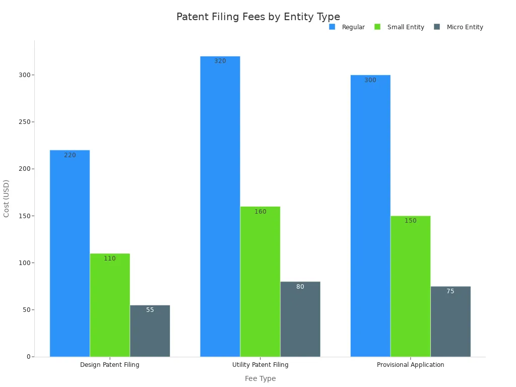
Filing a patent comes with costs you should understand. The following table shows USPTO filing fees:
Fee Type | Regular | Small Entity | Micro Entity |
|---|---|---|---|
Design Patent Filing | $220 | $110 | $55 |
Utility Patent Filing | $320 | $160 | $80 |
Provisional Application | $300 | $150 | $75 |
You also need to budget for attorney fees. Preparing a non-provisional patent application costs between $5,000 and $10,000. Contesting an examiner's rejection adds another $5,000 to $10,000. Timelines vary by patent type. Utility patents take 3 to 5 years to obtain. Design patents take about 22 months on average according to recent USPTO data for fiscal year 2023.
Trade secrets offer another layer of protection. Your pcb design contains valuable trade secrets you can protect. These include manufacturing processes, circuit designs, software source code, and business strategies. The Defend Trade Secrets Act (DTSA) provides a federal civil remedy for trade secret misappropriation. This fills a gap where only criminal penalties existed at the federal level.
Under current law, there are limited legal remedies for the theft or misuse of trade secrets. Federal law currently provides criminal penalties for trade secret misappropriation, but owners of trade secrets have lacked a federal civil remedy for the theft of their trade secrets. State laws provide a civil remedy, but the state courts lack the authority to act effectively against trade secret theft that crosses state and national borders. The Defend Trade Secrets Act empowers U.S. companies to protect their trade secrets in federal court, which is particularly relevant in today's world, where trade secret theft is often conducted across state or even national borders.
The DTSA creates a consistent, harmonized legal framework that works across state and national borders. This addresses the limitation of state courts in cross-border theft cases. Protecting your design with both patents and trade secrets gives you a stronger legal position.
Enforce NDAs with Manufacturers
Non-disclosure agreements are critical before you share your design files. Every manufacturer you work with must sign a strong NDA. Key clauses include non-disclosure terms, non-compete provisions, and penalty clauses for breach. You must specify exactly what information is confidential. This includes schematics, layout files, bill of materials, and firmware code. Always have a lawyer review the NDA before you share any design files. A well-written NDA gives you legal recourse if a manufacturer leaks your design. This step is essential to prevent pcba design theft at the manufacturing stage. Remember, every pcb you produce carries your intellectual property. You must protect it at every step.
Combining patent registration, trade secret protection, and strong NDAs creates a solid legal foundation. These measures give you enforceable rights and clear remedies. You start with these legal steps before you move to design obfuscation techniques. This layered approach makes it much harder to prevent pcba design theft.
PCB Design Obfuscation Techniques
Once your legal protections are set, you turn to the physical design. Obfuscation makes reverse engineering costly and slow. Attackers lose patience when they cannot spot key parts or follow circuit paths. You can use several proven methods to hide what your design really does.
Hide Critical Circuitry and Components
Defense contractors use specific ways to protect their boards. These methods make probing hard and raise the effort needed for X-ray checks. The table below shows the best approaches:
Technique | Core Mechanism | Protection Goal |
|---|---|---|
Active Tampering Protection | Parts placed inside with trace-resistance traits | Spots physical tampering in the field; makes probing tough |
Physical Unclonable Functions (PUFs) | Natural copper trace differences create unique random bit strings | Gives each PCB a unique ID to stop cloning |
JTAG Verification | Algorithmic checks of connected ICs | Lowers counterfeiting, cloning, and harmful changes |
MEMS Permutation Block | MEMS device swaps connections; additive manufacturing hides it behind ICs | Raises X-ray difficulty to block reverse engineering |
You can also add extra copper layers to hide signal paths. Remove reference labels from the silkscreen so attackers cannot tell part values. Erase chip markings by sanding or laser-etching part numbers. Use blind vias that link only certain layers, making surface tracing harder. These methods force thieves to spend a lot of time and money just to learn your board's basic layout.
Your pcb design gains a lot from stacking multiple obfuscation layers. Each method alone gives some cover, but together they form a maze that frustrates even skilled reverse engineers. Use as many of these as your budget and production limits allow.
Implement Firmware Encryption and Secure Boot
Your firmware holds valuable intellectual property that needs its own shield. Secure boot checks the integrity and authenticity of executable code at every startup step. It uses digital signatures or verified checks to ensure only approved, unchanged firmware runs. This directly blocks any altered firmware from starting. However, secure boot does not encrypt firmware, so it does not stop extraction by itself. It only prevents modified code from running.
You need extra steps to stop unauthorized access to your code:
Secure microcontrollers with built-in secure boot: These guard against unauthorized access to firmware or memory, stopping both extraction and changes.
Disabling debug interfaces (JTAG/SWD) after production: This stops attackers from reading memory contents or injecting harmful code.
Physical hardening (conformal coating): Makes probing or desoldering parts harder, deterring physical extraction attempts.
You should also set up regular firmware updates with cryptographic signing. Each update must carry a valid digital signature before the system accepts it. This stops attackers from installing changed versions of your code. Your printed circuit board becomes much harder to break when you pair secure boot with encrypted storage and locked debug ports.
Remember that firmware protection works best when you treat it as part of your whole pcb security plan. The same obfuscation ideas apply to code as to hardware. You hide key functions, obscure data flows, and make unauthorized access noticeable. Your pcb design should include these firmware protections from the start, not as an afterthought.
Secure PCB Manufacturing and Supply Chain
Your manufacturing partner holds your design files in their systems. That access creates risk. You must choose partners who treat your intellectual property as their own. The right fabricator protects your data with strong security measures and clear policies.
Partner with Trusted Fabricators
Start your search with certifications. These credentials show a fabricator's commitment to security. Look for suppliers who align with NIST 800-171 standards. This framework protects Controlled Unclassified Information from cyber threats. You also want partners pursuing CMMC readiness. The Cybersecurity Maturity Model Certification has three levels based on risk exposure. Higher levels mean stronger security practices.
IPC-1791D focuses on cybersecurity and CMMC implementation, giving confidence in product integrity, quality, supply chain risk management, and chain of custody for non-U.S. printed board design, fabrication, and assembly. IPC-1792 addresses the management and mitigation of cybersecurity incidents, securing the production, data exchange, and shipment process to prevent manipulation of software and hardware, ensuring products are built as intended by the original designer.
You should also conduct on-site audits before signing contracts. Verify these specific practices during your visit:
Network Segmentation: Confirm they isolate design, manufacturing, and supply chain networks with firewalls.
Access Control: Check that role-based permissions and multi-factor authentication protect your schematics.
Data Encryption: Ensure they encrypt files both at rest and during transfer using secure protocols.
Employee Training: Ask about their security education programs for all staff handling customer designs.
Your audit checklist should also cover NDA enforcement, data storage protocols, and clear terms about tooling ownership. A fabricator who passes these checks earns your trust. This diligence protects your pcb design from the moment you share your files.
Use Split Manufacturing and Serial Tracking
Split manufacturing spreads your design across multiple suppliers. One vendor produces certain layers of your board. Another handles different layers or components. No single partner sees your complete design. This method limits exposure and makes theft much harder.
You also need serial tracking for every unit you produce. Assign unique serial numbers to each pcb assembly. Use barcodes for instant location of any unit. Modern manufacturing ERP systems track each serialized board through its full lifecycle. You can trace a specific unit back to its exact manufacturing batch. This traceability helps you identify the source of any leak. When a counterfeit appears in the market, you can trace it to the responsible supplier.
Your pcb assembly process benefits from this layered approach. Split manufacturing prevents any one partner from copying your full design. Serial tracking gives you evidence if someone breaks your trust. Together, these methods create accountability throughout your supply chain.
Post-Production Physical and Legal Safeguards
Your board leaves the factory, but your protection work continues. Physical safeguards on each unit deter tampering. Legal enforcement deters copycats. Both layers work together to protect your investment.
Apply Tamper-Proof Coatings and Enclosures
Epoxy potting and conformal coatings create a hard barrier over sensitive components. Attackers cannot remove parts or probe traces without damaging the hardware. These coatings also show clear evidence of any break-in attempt. You can spot the damage right away.
Tamper-evident packaging adds another layer. Destructible vinyl labels, often called warranty void stickers, tear apart upon removal. They leave unmistakable proof of intrusion. You know instantly if someone opened your product.
Active tamper detection circuits take protection further. These circuits sense enclosure breaches through mechanical switches and conductive mesh. They detect voltage glitches, clock changes, and temperature shifts. Light sensors flag exposure of internal circuitry. When detection triggers, the circuit activates an erase function. It wipes encryption keys and sensitive memory before attackers extract anything.
The table below shows advanced tamper-proofing technologies for high-security applications:
Technology | Description |
|---|---|
Mesh sensors | Erase cryptographic keys if the mesh is physically breached |
Faraday cage layers | Screen-printed between PCB strata to prevent electromagnetic probing |
Self-destruct mechanisms | Triggered by intrusion attempts to destroy sensitive data |
Dedicated PCB layers | Entire layers designed to detect and respond to physical tampering in real-time |
Your pcb benefits from combining these methods. Thick solder mask conceals critical traces. Blacked-out components hide manufacturer identities. Blind vias reduce probing points. Each layer makes reverse engineering harder.
Monitor Market and Enforce Patents
Your legal protections only work when you enforce them. Monitor online marketplaces and trade shows for counterfeit copies. Search for products that match your unique design features. Set up alerts for suspicious listings.
When you find infringement, act quickly. Send a cease-and-desist letter first. This formal notice demands the infringer stop production and sales. Many cases end here without court action. If the infringer ignores your letter, escalate to patent litigation. Your registered patents give you standing in court. You can seek damages and injunctions against further production.
Your pcb design deserves this vigilance. Regular monitoring catches problems early. Swift legal action prevents small infringements from becoming widespread piracy. Together, physical safeguards and legal enforcement create a complete protection strategy.
No single tip guarantees complete safety.
You must use all the methods from this article together. They form a strong security setup. Start with legal steps. Register your patents and enforce NDAs first. Then use design hiding methods. Hide key parts and encrypt firmware. Pick trusted manufacturing partners. Use split manufacturing and serial tracking. Finally, add physical coatings and watch the market. This layered plan helps stop PCBA design theft. Your PCB needs protection at every step. Check your weak points today. Look at each layer of your security plan. Find gaps and fix them. Being proactive keeps your engineering work valuable. Use these tips as one full strategy. You build a strong wall against theft.
FAQ
What is the most important first step to protect your PCBA design?
Register your intellectual property before you share any files. File patents for circuit layouts and designs. Protect trade secrets with enforceable NDAs. This legal foundation gives you clear rights to stop theft before it starts.
How do design obfuscation techniques help prevent reverse engineering?
These methods make reverse engineering costly and slow. Extra copper layers hide signal paths. Removing chip markings stops part identification. Blind vias block surface tracing. All these techniques help prevent pcba design theft at the hardware level.
Can split manufacturing really stop a supplier from copying your board?
Yes. You give different layers to different suppliers. No single partner sees your complete design. This limits exposure. Combine this with serial tracking to trace any leak back to its source.
What should you do after finding a counterfeit copy of your product?
Act quickly. Send a cease-and-desist letter first. Many infringers stop at this point. If they ignore it, pursue patent litigation. Your registered patents give you standing in court to seek damages and stop production.
See Also
Essential Actions to Enhance PCBA Durability for Extended Use
Top Methods for Streamlining SMT Lines in PCBA Production
Expert Strategies for Perfecting BGA Assembly with Tested Methods
Starting Out: A Novice's Handbook for PCBA BOM Procurement
Comprehensive Overview of PCBA Fabrication for All Skill Levels
