PCB Layout Mistakes That Cause Robotic Soldering Problems

Your production line just stopped. A sudden spike in solder defects forces costly rework and missed deadlines. You might blame the machine, but the real culprit is often hidden in your board layout. Subtle pcb design mistakes create frustrating robotic soldering problems. These issues stem from six critical errors: pad and hole sizing, component placement, thermal relief, solder mask design, fiducial marks, and trace geometry. Use this checklist to audit your design files before manufacturing. You can prevent these issues by addressing design errors. Avoid weak joints by ensuring proper solder flow. Each decision directly impacts automated soldering reliability.
Key Takeaways
Use correct pad-to-hole ratios. Follow IPC standards. This prevents weak joints and solder starvation.
Match component footprints to datasheets. Generic footprints cause misalignment and tombstoning.
Add thermal relief spokes to ground pins. Large copper planes steal heat. Proper spokes prevent cold joints.
Maintain minimum solder mask webbing. Thin webbing peels and causes bridges. Use values from the table.
Place fiducial marks with proper size and clearance. Use global and local marks. Choose matte ENIG finish for good contrast.
Keep trace widths equal on both sides of pads. Unequal widths cause tombstoning from heat imbalance.
Balance copper density across layers. This prevents board warpage during soldering.
Pad and Hole Sizing Errors That Trigger Robotic Soldering Problems
Oversized Pads and Solder Starvation
Pad-to-Lead Ratio Guidelines
Your pad dimensions must match the component lead size. IPC standards recommend a pad diameter no more than 1.5 to 2 times the lead diameter for through-hole components. When you exceed this ratio, the pad becomes too large. The solder spreads across the copper surface instead of climbing the lead. This creates a starved joint with insufficient material. You see a flat, shallow fillet instead of a concave shape.
The joint lacks mechanical strength. This is one of the most common pcb design mistakes. Robotic soldering systems rely on consistent geometry to form reliable connections. Oversized pads disrupt that consistency. The machine cannot compensate for a layout that defeats capillary forces.
Capillary Action Failure Modes
Capillary action pulls molten solder up the lead during wave soldering. The narrow gap between the lead and the hole wall creates this force. When the pad is oversized, the gap widens. Capillary pressure drops significantly. The solder fails to wet the lead properly. You get incomplete wetting on the lead surface.
The resulting solder joint looks acceptable on top but has poor internal connection. This failure mode causes intermittent failures in the field. You cannot detect it with visual inspection alone. Robotic soldering systems cannot compensate for this design flaw. The machine follows your layout, and poor layout produces poor joints.
Undersized Holes and Blocked Solder Flow
Plating Voids and Weak Fillets
Undersized holes create a different set of problems. The lead cannot fit properly, or the clearance is too tight. The material struggles to flow through the annular gap. During the plating process, holes with tight tolerances develop voids in the barrel. These plating voids expose bare substrate material. The material cannot bond to the exposed area.
You get a weak fillet that passes initial testing but fails under thermal cycling. The joint cracks at the void location. This ranks among the frustrating robotic soldering problems. You think the machine is at fault, but the root cause is in your design files. These weak joints cause early failures in the field.
Via Wicking and Solder Drainage
Vias placed near through-hole pads can drain material away from the joint. The via acts as a wick, pulling molten material into its barrel. You end up with a starved solder joint on the primary pad. The fillet appears incomplete. The joint loses strength.
To prevent this, limit via placement within the thermal relief area. Use tented vias or plug them with masking. This maintains solder volume at the joint. Proper ground and power connections require careful planning here. You must balance electrical integrity with thermal needs. Bridges can form if vias are too close to pads. These bridges create short circuits. You catch them during inspection, but they add rework cost.
When you design your next pcb, verify pad-to-hole ratios. Check for nearby vias. Use standard dimensions from component datasheets. These small adjustments prevent major soldering problems. Your pcb layout directly affects joint quality and reliability.
Component Placement and Footprint Mistakes
Your component placement decisions directly affect robotic soldering reliability. Even a well-designed pcb fails if the footprint does not match the actual part. Issues in your pcb design cause common failures. Two errors create most of these issues: incorrect landing patterns and insufficient clearance for the soldering nozzle.
Incorrect Footprints and Landing Patterns
Mismatch with Component Datasheets
You must build your footprint from the specific component datasheet. Generic footprints cause trouble. Body size, lead pitch, and lead length vary between manufacturers. Sometimes they vary significantly within the same nominal package. A generic footprint built around an assumed body size leaves pads too short, too long, or misaligned with the actual leads.
This mismatch creates robotic soldering problems. The pick-and-place machine places the component offset from the pad center. Solder paste displaces during placement. During reflow, the component shifts. This shifting causes solder bridging between adjacent leads. You catch these bridges during inspection, but they add rework cost.
Tombstoning also results from footprint errors. One end of the component lifts during reflow. Uneven wetting force causes this. Differential melting times of solder paste on asymmetrical pads create the imbalance. Your footprint design controls this balance. Get it wrong, and the joint fails.
Impact on Solder Paste Deposition
The footprint controls solder paste deposition. The stencil aperture aligns with the pad. If the pad is too short, the paste deposit is insufficient. You get a weak solder joint with inadequate coverage on the lead. If the pad is too long, excess paste spreads beyond the component. This creates balls or bridging.
Your paste deposition volume must match the pad geometry. Each component type requires specific paste volume calculations. The footprint determines the stencil design. A mismatch at the footprint level propagates through the entire soldering process. You cannot fix it with machine adjustments.
Insufficient Nozzle Clearance and Shadowing
Minimum Distance from Tall Components
Nozzles need physical clearance to operate. Tall components create interference. For selective wave processes, components exceeding 12mm in height require more than 8mm clearance from the solder pads. This distance ensures the nozzle reaches the joint without touching the component body.
You must check this clearance during your pcb layout. Place tall components at the board edge or in dedicated zones. Group them away from fine-pitch connectors. Your placement strategy determines whether the nozzle can access every joint.
Uneven Heat Distribution from Dense Placement
Dense placement creates a shadowing effect. A tall component blocks the dominant heat transfer path. This path is either convective airflow or infrared radiation. The shadow prevents the paste on the adjacent low-profile part from reaching its full reflow temperature.
The result is a cold joint or incomplete reflow. You see voids in the solder joint. The joint lacks strength. Diagnostic thermal profiling on the shadowed component measures the temperature deficit. You can correct this by repositioning the tall component upstream in the oven direction. Increase spacing to at least 2 times the height difference between components. This guideline comes from IPC-7530B. Your pcb design must separate tall and short components.
Your component placement must account for these thermal effects. Signal integrity and power distribution matter. But mechanical and thermal clearance matters equally for reliable joints. High-speed signals require careful routing around tall components. Ground planes help with heat distribution but need proper thermal relief. Signal degradation from cold joints creates reliability issues.
Thermal Relief Deficiencies Causing Soldering Defects
Your ground pins connect to large copper planes. Without proper thermal relief, those planes act as massive heat sinks. They pull heat away from the joint faster than the soldering system can supply. The joint never reaches the liquidus temperature. You get a cold solder joint.
The Heat Sink Effect of Large Copper Areas
Large copper planes draw thermal energy away from the through-hole barrel. The solder wave delivers heat, but the copper plane dissipates it laterally. The contact patch limits heat transfer. Simply increasing the soldering power does not help. The joint cannot reach the required temperature. This heat dissipation creates cold joints that lack mechanical strength. These joints fail during testing. A poor pcb design causes this problem.
Why Robotic Soldering Needs Rapid Heat-Up
Robotic soldering systems rely on precise temperature profiles. They deliver heat in a controlled window. The solder must reach the liquidus temperature quickly for proper flow to occur. When a large copper plane acts as a heat sink, the temperature rise slows. The solder does not flow. You get incomplete wetting on the lead surface. The joint looks acceptable but fails during thermal cycling. Your design must account for this heat loss.
Missing or Inadequate Thermal Relief Spokes
Thermal relief spokes create a controlled path for heat. They restrict the copper connection to the plane. This limits heat loss during soldering. Without adequate spokes, the plane continues to drain heat. This is a common mistake in pcb design.
Standard Spoke Configurations
You need specific configurations for different components. The table shows recommended values.
Component Class | Spoke Width | Air Gap |
|---|---|---|
Fine-pitch passives (0402, 0603) | 0.10 to 0.20 mm (4 to 8 mil) | 0.20 to 0.30 mm (8 to 12 mil) |
General SMD (0805, SOT-23, SOIC) | 0.20 to 0.30 mm (8 to 12 mil) | 0.25 to 0.40 mm (10 to 16 mil) |
Through-hole pins on a plane | 0.30 to 0.50 mm (12 to 20 mil) | 0.40 to 0.60 mm (16 to 24 mil) |
Any pad above 3 A continuous | None, direct connect | Not applicable |
Altium defaults to 0.2 mm (8 mil) spokes and clearance for most parts. KiCad defaults to 0.508 mm (20 mil) for both. These defaults provide a starting point. Adjust based on your needs.
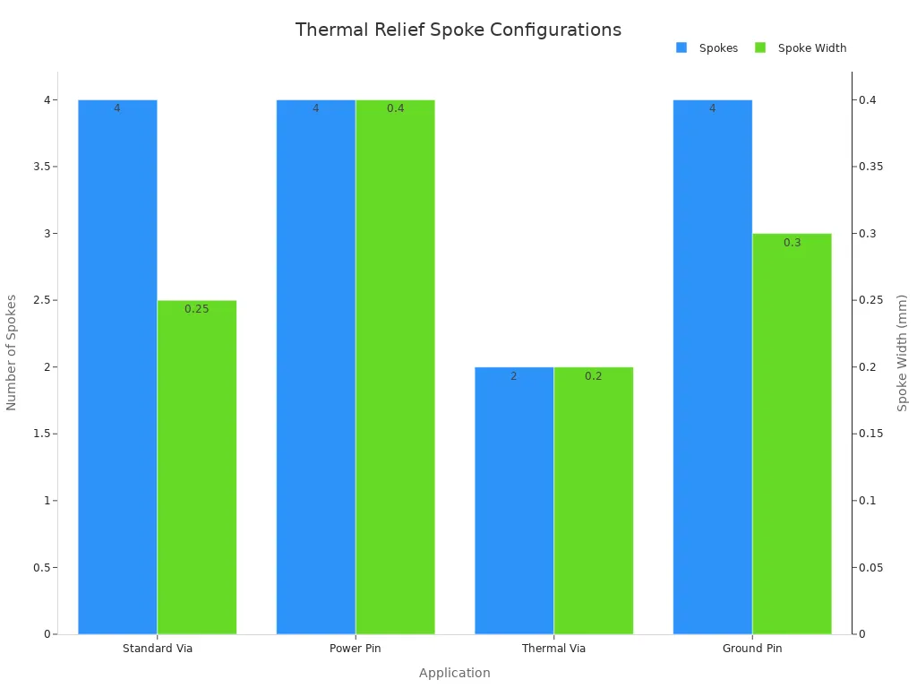
The number of spokes matters. Four spokes offer good solderability for standard vias and ground pins. Two spokes provide excellent solderability for thermal vias. Power pins need four spokes at 0.4 mm width, though solderability becomes marginal.
Balancing Electrical and Thermal Needs
Spoke width creates a trade-off. Wide spokes offer lower resistance and better current handling. They also reduce thermal relief, making the process harder. Narrow spokes improve thermal relief and ease soldering. But they increase resistance and current density. The solder joint quality depends on this balance.
For a 0.25 mm microvia pad, keep spoke width at 0.10 to 0.12 mm. This maintains high thermal resistance for solderability. The DC resistance increase stays under 5 mΩ on 1/2 oz copper. This is acceptable for most power and ground nets.
Your power and ground plane layouts must balance these needs. Check current requirements. If a pad carries over 3 A continuous, do not use thermal relief. Connect directly to the plane. For lower current signals, use the standard configurations.
This is one of the most common robotic soldering problems. The pcb design looks correct. But the thermal relief settings cause poor joints. Always verify your pcb thermal relief settings before manufacturing.
Solder Mask and Silkscreen Errors Leading to Common PCB Soldering Problems
Your solder mask and silkscreen layers can create hidden defects that disrupt automated assembly. These layers seem cosmetic, but they directly affect joint quality. Poor mask coverage causes bridges between pads. Silkscreen overlapping pads blocks solder adhesion. Sharp trace angles trap corrosive chemicals. Each issue contributes to common pcb soldering problems.
Solder Mask Slivers and Bridging Risks
Minimum Solder Mask Webbing Width
Solder mask webbing is the thin strip of mask material between adjacent pads. When this strip becomes too narrow, it peels away during processing. The exposed copper allows solder to flow across the gap. You get bridges that short-circuit your board.
The minimum webbing width depends on your copper weight and ink type. Standard green inks require wider spacing on heavier copper. Pigmented inks like black and white need even more clearance because their chemistry flows differently.
Process & Material Configuration | Finished Copper 1 oz (35 μm) | Finished Copper 2 oz (70 μm) |
|---|---|---|
Standard Inks (Green, Red, Yellow, Blue, Purple) | Minimum Pad Spacing ≥ 0.10 mm (4 mil) | Minimum Pad Spacing ≥ 0.20 mm (8 mil) |
Pigmented Inks (Matte/Glossy Black, White) | Minimum Pad Spacing ≥ 0.13 mm (5.1 mil) | Minimum Pad Spacing ≥ 0.20 mm (8 mil) |
These values come from JLCPCB manufacturing guidelines. Altium recommends a minimum web of approximately 3 mils for the mask to adhere properly. Follow these limits to prevent mask peeling and subsequent bridges.

Silkscreen Interference with Vision Systems
Keeping Silkscreen Clear of Pads and Fiducials
Silkscreen ink overlapping pads creates a serious problem. The ink contaminates the solderable surface. Solder cannot wet the pad properly. You get weak connections that fail under stress.
Silkscreen covering a 0.5 mm diameter pad prevents proper solder adhesion. The ink blocks the solder from bonding to the copper. This defect directly affects robotic soldering quality.
The conflict is not merely aesthetic. Component designators printed over pads obscure critical areas. The vision system cannot locate the pad center. Placement accuracy drops. Rework costs rise.
Fiducial marks require special attention. Maintain a keep-out diameter of 2–3 times the fiducial diameter. Keep this zone completely free of silkscreen, text, copper traces, and solder mask encroachment. Never use silkscreen-only fiducials. They register less accurately than copper features. Avoid placing vias or text inside the keep-out zone. These features interfere with reliable centroid detection.
Acid Traps from Acute Trace Angles
Rerouting to Avoid Sharp Corners
Acute angles in copper traces create acid traps. During etching, chemicals collect in the narrow corner. The neutralization and washing steps cannot fully remove them. Residual chemicals slowly corrode the copper over time.
This corrosion increases trace resistance. Eventually, you get a virtual open connection. Short-circuit faults become difficult to troubleshoot. The long-term reliability of your assembly suffers.
You can prevent acid traps with simple routing changes:
Use 45-degree angles instead of sharp 90-degree turns. This allows better chemical flow during etching.
Maintain minimum spacing of 6 mils between traces and pads. This prevents chemical buildup.
Check for acute angles using design software tools that automatically flag potential acid traps before production.
Chamfering cuts off the sharp corner of a right-angle trace. This creates a 45-degree angle and reduces signal reflections. Curved traces replace sharp right angles with smooth arcs. This maintains signal integrity in high-speed designs. Eliminate all angles less than 90 degrees. These simple adjustments prevent corrosion and keep your solder joints reliable.
Your pcb design must account for these mask and silkscreen details. The soldering process depends on clean, unobstructed pads. The vision system depends on clear fiducials. The copper traces depend on proper geometry. Address these issues before manufacturing to avoid robotic soldering problems.
Missing Fiducial Marks as a PCB Design Mistake
Fiducial marks are non-negotiable for robotic soldering systems. Without them, alignment fails. The machine cannot determine the board's exact position. This causes misaligned solder joints and costly rework.
The Role of Fiducials in Automated Alignment
Your machine's vision system needs predetermined optical references. Without fiducial-based vision correction, placement accuracy can drift by 100 to 200 micrometers. Board loading variations cause this shift. When you implement fiducial recognition properly, the error drops to less than 25 microns. This precision matters for fine-pitch components. A 0.5mm pitch QFP or a 0.4mm pitch BGA depends on this accuracy.
Accurate fiducial placement reduces misalignment errors. A 1% error rate on a batch of 10,000 boards creates 100 defective units. Each repair can cost $50 or more. Fiducials prevent this waste. They allow machines to recognize board orientation quickly. This can increase throughput by up to 20% in high-volume production runs.
Global vs. Local Fiducial Placement
You need two types of fiducial marks. Global fiducials align the entire board. Local fiducials correct for distortion near fine-pitch components.
Aspect | Global Fiducial Marks | Local Fiducial Marks |
|---|---|---|
Primary Function | Align the entire PCB to the machine's coordinate system. | Correct alignment for high-precision components (pitch ≤ 0.5mm). |
Placement | Minimum of two, recommended three, in an 'L' configuration. | Two marks diagonally opposite the component's land pattern. |
Correction Scope | Corrects for global X, Y, and rotational offsets. | Corrects for local FR-4 material instability. |
Usage Context | Required for all SMT boards. | Used for fine-pitch components. |
The machine detects the global marks first. It aligns the board by compensating for rotation or positional shift. The stencil aligns with the fiducials to apply solder paste accurately. Pick-and-place machines then position components with precision.
Poor Fiducial Contrast and Placement
Your fiducial marks must provide high contrast against the board background. The vision system needs a clear, distinct target. Poor contrast causes recognition failures.
Minimum Size and Clearance from Board Edge
Your fiducial marks must meet specific size requirements. The minimum copper diameter is 1.0 mm. An acceptable range spans 0.8 to 1.5 mm. The solder mask opening must be 2.0 mm for a 1.0 mm copper pad. Maintain a minimum edge clearance of 5.0 mm from the board edge. Keep a clearance zone of 2 to 3 mm radius around the fiducial. This zone must be free of traces, vias, or silkscreen.
Avoiding Glare and Reflection
Glare prevents the vision system from recognizing the fiducial. You need a matte surface finish to prevent this. The area surrounding the fiducial must remain completely exposed. Keep it free from mask covering. The surface finish matters. Fiducials with an Electroless Nickel Immersion Gold (ENIG) finish achieve a significantly higher recognition rate in low-light environments. This compares to a HASL finish. Selecting ENIG over HASL can directly improve vision system reliability. Your pcb design must account for these details. The soldering process depends on clean, visible fiducials. The robotic soldering system cannot compensate for poor fiducial design. Address these issues before manufacturing.
Trace Geometry and Copper Balance Issues
Your trace geometry directly affects joint quality. Unequal trace widths connected to the same pad create thermal imbalance. One side heats up faster than the other. This imbalance causes tombstoning defects during reflow soldering. The component lifts on one end. This pcb design mistake is preventable.
Unequal Trace Widths and Heat Distribution
The "Necking" Effect on Solder Flow
When you connect a wide trace to a small pad, the solder spreads across the copper surface. This excessive spreading creates beads. The joint lacks the proper fillet shape.
Wide traces connected to small pads cause excessive solder spreading during reflow, increasing the risk of solder beads and uneven joint formation. Similarly, small passive components connected to large copper areas experience uneven heat dissipation, with one side cooling faster than the other, leading to tombstoning, weak solder joints, or component displacement.
The necking effect occurs when you narrow a trace between two wide sections. The narrow section limits current flow. It creates a hot spot during operation. This hot spot affects the joint during reflow. The temperature difference causes uneven wetting. The solder cannot flow properly.
Your signal traces need consistent width. This maintains signal integrity. Uneven trace width creates impedance discontinuities. These affect signal quality. For high-speed signals, this problem becomes critical. The mismatch causes signal reflections. These degrade signal integrity.
Power and ground traces need careful planning. A power trace with inconsistent width creates voltage drop. Ground traces need low impedance for return paths. Wide traces provide lower impedance. But wide traces also affect heat distribution during soldering. Your design must account for this trade-off.
Copper Slivers and Board Warpage
Minimum Copper-to-Edge Spacing
Copper slivers are narrow strips of copper. They can break under thermal stress during the soldering process. Maintain minimum spacing from the board edge. The recommended minimum copper-to-edge spacing is 0.5 mm for inner layers. For outer layers, use 0.3 mm. Good pcb layout prevents this problem.
Balancing Copper Density Across Layers
Uneven copper distribution across layers causes board warpage. The board bends toward the lighter copper side during heat cycles. This warpage creates alignment problems.
Condition | Board Warpage (Typical) |
|---|---|
Without copper thieving | 1.0-1.5% bow/twist |
With copper thieving | Less than 0.5% |
Copper grows about four times faster than standard board base material. This growth gap creates board warpage because heat cycles push the board to bend toward the lighter copper side.
You need to balance copper density across all layers. Copper thieving adds dummy copper to empty areas. This reduces warpage to less than 0.5%. Your power and ground planes need careful distribution. A ground plane on one layer needs a matching copper fill on the opposite layer.
Signal layers also need balanced copper distribution. Spread your signal traces evenly across the layer. Avoid clustering traces in one area. This prevents localized copper density variations. For high-speed signals, you need controlled impedance. This requires specific trace width and spacing. Plan your layer stack-up to balance copper density while maintaining signal integrity.
Your trace width and spacing decisions affect both assembly quality and signal performance. Consistent trace geometry prevents thermal imbalance. Balanced copper distribution prevents warpage.
These six pcb design mistakes share one root cause: unpredictability. Robotic soldering demands consistency. Your layout must deliver identical conditions for every joint. Oversized pads, missing thermal relief, or poor fiducials create variables the machine cannot correct. Each flaw produces weak joints or cold solder connections.
You can prevent these problems. Run rigorous Design Rule Checks before release. Share your files with manufacturing engineers early. Their feedback catches subtle errors your software misses. A perfect solder joint starts with a predictable design.
Send your layout for a free DFM review. Comment below with your own soldering challenges. Your next board deserves this attention.
FAQ
How do I check my pad-to-hole ratios before sending files to manufacturing?
Open your component datasheets and compare lead diameters against your pad dimensions. IPC standards recommend pad diameters no more than 1.5 to 2 times the lead diameter for through-hole parts. Your CAD software can flag violations automatically during Design Rule Checks.
What is the minimum solder mask webbing I should maintain?
For standard green ink on 1 oz copper, keep pad spacing at 0.10 mm or greater. Pigmented inks like black or white require 0.13 mm minimum spacing. Heavier 2 oz copper needs 0.20 mm spacing regardless of ink type. These values prevent mask peeling and solder bridging.
Can I skip thermal relief for low-current connections?
No. Thermal relief spokes control heat flow during soldering. Without them, large copper planes drain heat away from the joint. The solder never reaches liquidus temperature. You get cold joints that fail under thermal cycling. Always use proper spoke configurations for connections carrying less than 3 A.
How many fiducial marks does my board need?
You need at least two global fiducials, ideally three arranged in an L-shape. Fine-pitch components with 0.5 mm pitch or smaller require additional local fiducials placed diagonally opposite each other. These marks enable the vision system to correct for board distortion and placement errors.
What causes tombstoning during reflow soldering?
Unequal trace widths connected to the same pad create thermal imbalance. One side heats faster than the other. The solder on the faster side melts first and pulls the component upward. Keep trace widths consistent on both sides of small passive components to prevent this defect.
How close can vias sit to through-hole pads?
Vias placed too close to pads wick solder away from the joint. This creates starved connections with incomplete fillets. Keep vias outside the thermal relief area or use tented vias to block solder flow. This preserves solder volume at the primary joint.
Should I use ENIG or HASL finish for my fiducials?
ENIG finish provides better contrast for vision systems. Fiducials with ENIG achieve significantly higher recognition rates in low-light environments compared to HASL. The matte surface reduces glare and reflection. Choose ENIG for boards that rely heavily on automated optical alignment.
What copper-to-edge spacing prevents board damage?
Maintain 0.5 mm minimum spacing from the board edge for inner layers. Use 0.3 mm for outer layers. This prevents copper slivers from breaking under thermal stress during soldering. Proper spacing also reduces the risk of board warpage from uneven copper distribution.
See Also
Steer Clear Of Frequent Errors In Ball Grid Array Assembly
Typical Flaws In Surface Mount PCB Assembly And Their Prevention
Key Considerations For Surface Mount Assembly Of Rigid-Flex Boards
Achieve Expertise In BGA Assembly Using Effective Methods And Tricks
Critical Technical Concerns For VIPPO PCBs During Surface Mount Assembly
