Key Parameters in Multilayer PCB Pressing Explained
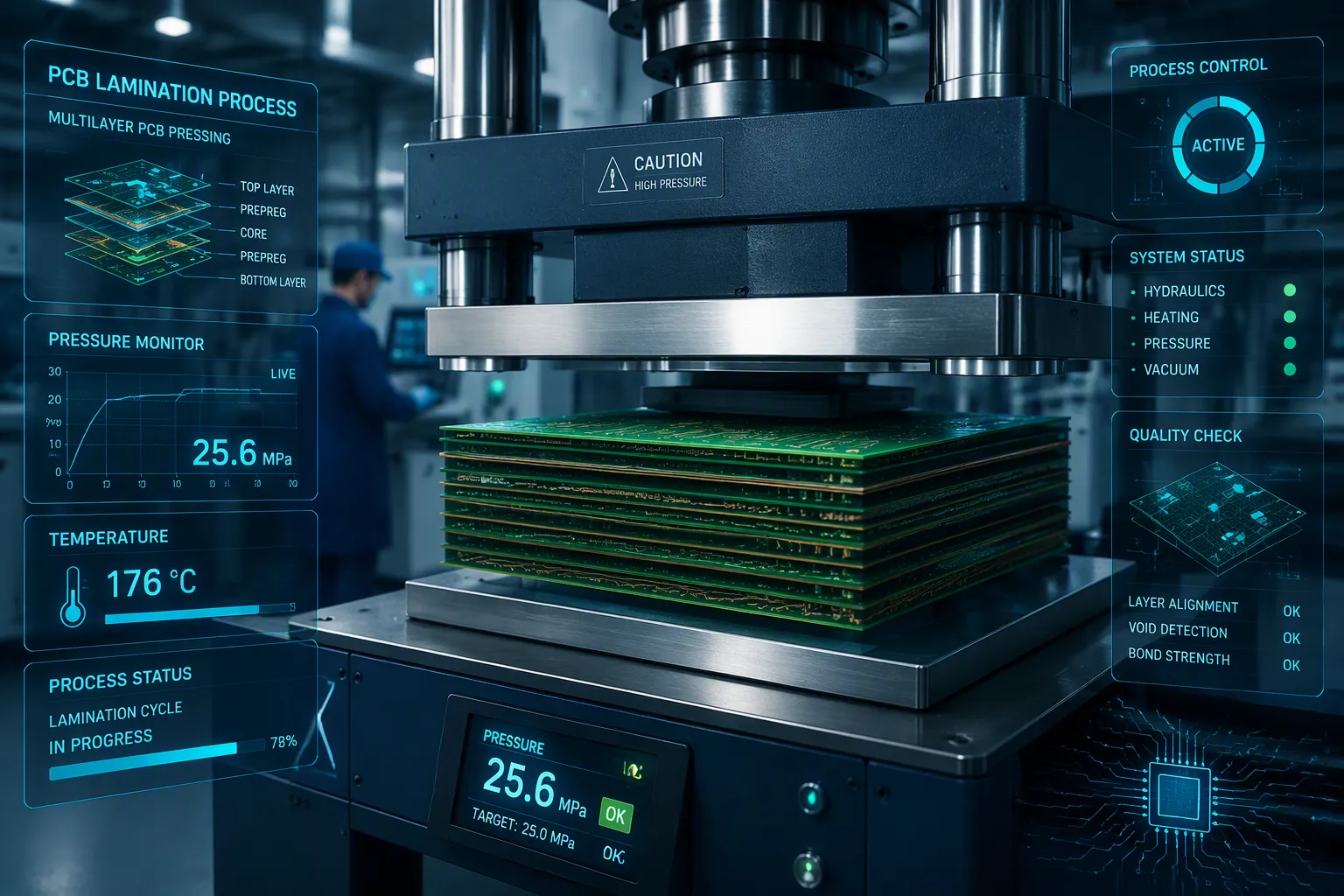
The lamination step decides how good and reliable your multilayer PCB will be. You manage this process with four Key Parameters: temperature, pressure, time, and material stack-up. Each parameter affects the others, creating a careful balance.
Temperature controls how resin flows and cures. Pressure removes air pockets and joins layers together. Time lets chemical reactions finish properly. Your material stack-up design changes how heat and pressure spread across the board.
The main challenge is tuning these settings together. You must stop defects like delamination, layer shifting, and warping. Keep moisture away from materials before pressing. Store boards below 30°C and 60% humidity. Keep stack-ups balanced to avoid warping. Your circuit board design choices directly affect manufacturability and yield.
Key Takeaways
Temperature, pressure, time, and material stack-up all work together to decide how good the PCB turns out.
Control the speed of temperature changes and the time spent at steady heat levels to stop air pockets from forming and make sure the material cures evenly.
Start with light pressure, then apply full pressure. This prevents resin starvation and helps create a strong bond.
Control the gel time and cure window to stop layers from separating and to make sure the resin bonds correctly.
Balance all settings to cut down on flaws like peeling and bending, boosting output and dependability.
Key Parameters for Temperature
Temperature is the most important control in the multilayer pressing process. You must manage heat carefully because it drives resin flow, chemical curing, and final bond strength. The typical range for standard FR-4 materials sits between 180°C and 200°C. Your exact target depends on the resin system and the specific grade of material you use.
FR-4 Grade | Lamination Temperature Range |
|---|---|
Standard (hot plate) | 180°C – 200°C |
Optimal (standard grades) | 180°C – 190°C |
High-Tg variant | ~200°C |
Ramp Rates and Soak Zones
You should heat the stack at a controlled rate of 2–4°C per minute. This gradual rise lets the epoxy resin soften evenly across all layers. A faster ramp traps gases inside the board, creating voids that weaken the final product. Slow heating also prevents thermal shock, which can crack thin dielectric materials.
The soak zone serves a different purpose. During this phase, you hold the temperature steady so heat spreads uniformly through the entire stack. Thick copper planes and dense circuit patterns heat slower than thin prepreg areas. Without a proper soak, some regions reach curing temperature early while others lag behind. This uneven heating causes incomplete bonding and internal stress.
Inadequate Temperature Control: Temperature control is critical during the curing of the resin used in lamination. Incorrect temperature profiles can lead to incomplete bonding and void formation. Similarly, trapped gases result from incorrect temperature profiles that cause incomplete encapsulation. The lamination profile must be set correctly before initiating the process to minimize void formation.
Peak Temperature and Cooling
Your peak temperature typically reaches 170°C to 200°C, depending on the material specification. At this point, the resin completes its cross-linking reaction. You must hold this temperature long enough for the chemical reaction to finish across every layer of the circuit board. Short holds leave the resin under-cured, which reduces the integrity of the finished board.
Cooling demands equal attention. You should reduce the temperature at 2–4°C per second during the cooling stage. Rapid cooling creates thermal expansion mismatches between copper and dielectric materials. These mismatches cause warping or delamination over time. A controlled cooling rate lets the board solidify without internal stresses, improving long-term performance and signal quality.
The entire temperature profile—ramp, soak, peak, and cool—works as one system. Each phase affects the next. When you master these key parameters, you improve the quality of every multilayer circuit board you produce. Your manufacturing processes become more predictable, and your final products deliver better signal performance across all layers.
Pressure Settings in Multilayer PCB Lamination
Pressure is one of the main settings you control during this multilayer manufacturing process. It works with heat to push out air and join the layers together. You use pressure in two steps. The first step uses low pressure. The second step uses high pressure.
Kiss Pressure and Resin Flow
Kiss pressure is between 15 and 50 PSI. You use it while the stack heats up. The heat makes the prepreg resin soft. The low pressure keeps the stack from moving. It stops the resin from flowing out too quickly. Using high pressure too soon causes resin starvation. Your circuit board then has weak spots and empty spaces.
The kiss pressure helps the resin spread evenly across the multilayer board. It fills gaps between copper traces and dielectric materials. Without proper kiss pressure, air gets trapped. These empty spaces lower the mechanical strength of the pcb. They also hurt signal quality in high-speed circuits. You must control this first pressure carefully. It decides how well the final bond turns out. The resin moves into the gaps and forms a strong bond.
Full Pressure, Dwell Time, Bonding
After the resin gels, you raise the pressure. Full pressure ranges from 200 to 400 PSI. Most presses use around 300 PSI. Some advanced presses go up to 500 PSI. This high pressure pushes the stack together. It removes any leftover air pockets. It also makes sure the resin cross-links fully.
You keep this full pressure during the dwell time of the curing process. The dwell time lasts until the resin cures completely and keeps the stack in tight contact. Without tight contact, the board can separate later. The dwell time also sets the final thickness of the multilayer circuit boards. Too much or too little pressure changes the board's impedance. You must watch thickness control during the lamination process.
The mix of pressure and time creates a strong, dependable board. Thicker boards with many copper layers need higher pressure. Thinner boards with fewer layers need lower pressure. Your manufacturing processes must handle these differences. The pcb manufacturing cycle depends on this balance.
The whole pressure control process decides how well your lamination works. When you handle these settings correctly, you make a circuit board with great alignment and mechanical strength. Your signal performance improves across all layers. Your manufacturing step becomes more repeatable and cost-effective. The multilayer circuit depends on these settings to work properly.
Time and Cycle for Multilayer PCB Manufacturing Process
The key parameters work together during the lamination process. Time is the third you control. It works with temperature and pressure to determine the final quality of your circuit board. You must manage two main time windows. The first is the gel time and cure window. The second is the total cycle duration.
Gel Time and Cure Window
The gel time marks the moment when the resin changes from a liquid to a solid state. During this phase, the resin flows and fills gaps between layers. The gel point temperature and dwell time depend on the specific prepreg material and must be set according to the manufacturer's datasheet.
Parameter | Value |
|---|---|
Gel Point Temperature | Varies by prepreg material |
Dwell Time at Gel | Per manufacturer's specification |
The cure window follows the gel phase. During this time, the resin cross-links fully. You must set the cure time to the nominal point for your specific resin system. If you use too much time, the resin becomes overcured and brittle. This brittleness causes rough hole walls during drilling. The rough walls compromise the integrity of via connections in your pcb. If you use too little time, the resin remains undercured. Undercured resin creates excess smear during drilling. It also leads to delamination during later thermal processes like soldering. Both overcuring and undercuring degrade the electrical and mechanical reliability of your circuit board.
Total Cycle Duration and Throughput
The total press cycle time for multilayer circuit boards ranges from 4 to 6 hours. This includes the lamination phase and the cooling phase.
Process Phase | Duration Range |
|---|---|
Lamination (heat & pressure) | Varies |
Cooling (after lamination) | Varies |
Total press cycle time | 4 – 6 hours |
The average lamination cycle time for your manufacturing process is 4 to 6 hours per cycle. Your stack-up complexity directly affects this duration. When manufacturing multilayer pcbs, you must account for each cycle. When you manufacture a board with many layers, you may need sequential lamination cycles. Each additional cycle adds significant time to the production schedule. Sequential lamination requires inner layer fabrication with thickness control, registration, pressing, and inspection for each cycle. These steps compound the total duration.
The average lamination cycle time for multilayer PCBs is 4 to 6 hours per cycle.
You must balance cure time with throughput. Shorter cycles increase output but risk incomplete curing. Longer cycles ensure proper bonding but reduce the number of boards you can produce each day. Your stack-up complexity also affects the performance of the final board. Asymmetric multilayer stacks cause warpage and uneven thickness. High layer counts require more controls and inspections. These factors extend the total time for printed circuit board manufacturing.
The total lead time for a prototype of printed circuit board manufacturing is typically a few weeks. For volume production of 1000 units or more, the lead time grows to several weeks. Each additional lamination cycle increases production cost compared to traditional designs. These costs come from the extra process steps and the higher risk of defects in your pcb.
Your understanding of these time settings helps you optimize the multilayer pcb manufacturing process. You must track the gel time, cure window, and total cycle duration. When you manage these settings correctly, you achieve better yield and reliability. Your circuit board manufacturing becomes more predictable and cost-effective. The final board shows better performance and signal integrity.
How Key Parameters Impact Common Defects
Your control over temperature, pressure, and time directly determines whether defects appear in your finished multilayer boards. Understanding how these key parameters interact helps you prevent costly failures before they happen.
Delamination from Temperature and Pressure
Delamination happens when layers pull apart from each other. Temperature changes can trigger this failure through uneven expansion. When heat shifts quickly or unevenly, copper and dielectric materials grow at different rates. This stress pulls layers apart at their weakest points. Pressure changes cause a different issue. Too little clamping force stops resin from flowing properly into gaps. Weak spots stay unfilled, creating places where separation can start.
Factor | Mechanism | Direct Consequence |
|---|---|---|
Temperature deviation | Rapid or uneven temperature changes | Stress from uneven expansion leads to layer separation |
Pressure deviation | Insufficient clamping force | Resin cannot fill voids, leaving weak bond interfaces |
Your ramp rate plays a key role in stopping these failures. Heat applied too fast turns prepreg resin into liquid that squeezes out, leaving the board resin-starved. Heat applied too slowly causes resin to cure before filling gaps between copper traces. Both scenarios create poor bonding. You can fix this by embedding thermocouples to monitor actual board temperature. This approach keeps resin in its best viscosity range throughout the entire lamination cycle, ensuring void-free encapsulation.
Bow, Twist, and Thickness Control
Bow and twist deform your circuit board after lamination. Uneven copper distribution causes one side to shrink differently than the other. Asymmetrical layer stack-ups create internal stress that warps the board. External processes like soldering and handling add further deformation risk.
Your multilayer thickness parameters determine final board dimensions. Even pressure distribution across the stack ensures consistent thickness throughout. Hydraulic lamination presses excel at this because they apply uniform pressure across the entire surface. This uniformity supports both layer alignment and void prevention.
The key parameters you set during pressing affect every aspect of final quality. Proper cross-plying of prepreg layers prevents weave distortion. Balanced copper distribution across layers reduces warpage risk. Under-cured inner layers create hidden weaknesses that appear during later assembly steps.
Your manufacturing processes must account for these variables. When you control ramp rates, manage kiss-to-full pressure transitions, and respect gel time windows, you achieve better alignment and signal integrity. The final multilayer circuit boards show improved performance and fewer signal integrity issues. Your circuit design choices directly influence manufacturability, so consider thickness parameters early in the design phase. Mastering these settings leads to higher yield, better reliability, and lower cost for your multilayer manufacturing process.
You must tune temperature, pressure, time, and materials together. Each parameter affects the others. Higher temperature lowers resin viscosity, letting it flow into gaps. Pressure then consolidates the layers. Sustained time completes the cross-linking cure. Follow your material supplier's processing guidelines for the best results.
Optimization Outcome | Improvement |
|---|---|
Delamination defects | Significant reduction |
Layer registration | Improved tolerance |
Verify material specifications before pressing. Use IPC-4101 base material standards and appropriate test methods. Factory insights recommend pilot runs for new designs.
Comprehensive optimization stabilizes dielectric thickness and impedance performance.
Mastering these parameters delivers higher yield, better reliability, and lower manufacturing cost.
FAQ
What happens if you raise the temperature too quickly during lamination?
Heating too fast traps gas inside the board. This creates air pockets that make the bond weak. It can also crack thin dielectric layers. Instead, use a steady ramp rate of 2–4°C per minute.
Why do you use a low kiss pressure before applying full pressure?
Using full pressure too early squeezes resin out of the stack. This leads to resin starvation. Kiss pressure at 15–50 PSI lets resin spread evenly and fill gaps. Then full pressure at 200–400 PSI presses the layers together.
What causes bow and twist in a finished multilayer board?
Uneven copper distribution creates stress inside the board. Asymmetric stack-ups cause one side to shrink more than the other. A controlled cooling rate of 2–4°C per second stops warping. Balance your layer design from the beginning.
What is gel time and why does it matter for your process?
Gel time is when prepreg resin changes from liquid to solid. The temperature and dwell time depend on the specific prepreg material and should be set per the manufacturer's guidelines.
How should you store prepreg and core materials before pressing?
Keep materials below 30°C and 60% humidity. Moisture causes voids during lamination. Proper storage keeps resin behavior consistent. It also improves the final bond quality and reliability of your board.
See Also
Achieving Peak Performance Through Flexible PCB Assembly
Comprehensive PCBA Manufacturing Guide for All Skill Levels
Combining SMT and DIP Assembly for Superior Mixed Technology PCBs
