IoT Device PCBA Manufacturing Challenges
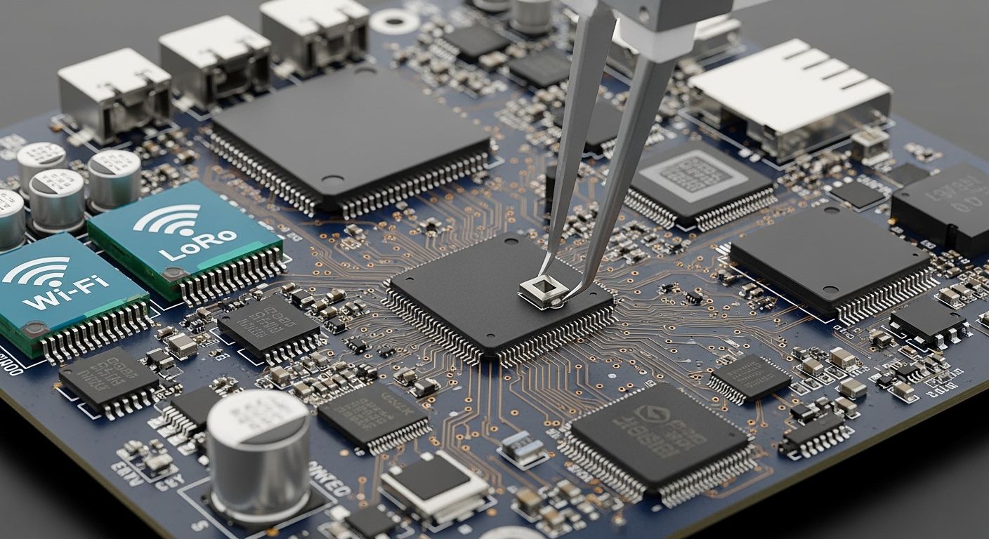
Engineers face tough PCBA manufacturing delays when building hardware for the Internet of Things. Modern IoT gadgets cram high-power microcontrollers, tiny sensors, and active wireless antennas into small cases. This large feature count raises overall PCB routing difficulty and creates strict space limits.
Designers must handle thermal management and RF layout issues early in the engineering process. Bad trace placement hurts signal integrity, while unmanaged heat damages inner parts. High-frequency routing needs careful shielding protocols to stop cross-talk near processing nodes. Early Design for Manufacturability checks prevent yield drop-off during prototype-to-mass-production shifts. Smart early planning ensures smooth growth during full-scale printed circuit board assembly.
Key Takeaways
Designers test software early to fix signal mistakes and save money on rebuilding circuit boards.
Engineers use microvias and thermal via arrays to cool tiny parts inside small sealed cases.
Quality inspectors use 3D X-ray scans to find hidden solder defects and boost board reliability.
Factory teams perform early building checks to lower production costs and grow assembly smoothly.
Technical PCBA Manufacturing Challenges in IoT Devices
Engineers handle huge design problems when building small circuit boards for new IoT gear. Making compact hardware means packing many parts onto tiny boards while keeping them reliable and working well.
Miniaturization and High-Density Interconnects
Engineers must balance tiny board space against heavy part counts during early component placement. New IoT gear crams main processors, sensors, and power circuits into packed multi-layer designs. Shrinking an industrial IoT sensor board footprint from 50×50 mm down to 40×40 mm makes the layout much harder. Fine-pitch components, ball grid arrays, and double-sided placement cause common mistakes like tombstoning, solder bridging, cold joints, and BGA voiding.
Challenge in IoT multi-layer PCBA | Documented evidence from the case study |
|---|---|
EMI sensitivity | High EMI interference reduced to minimal levels after stackup optimization. |
Signal integrity | Board performance improved from moderate to excellent levels. |
Thermal management | Heat dissipation addressed using optimized stackup and laser-drilled vias. |
Compact footprint | Overall device size reduced from 50×50 mm to 40×40 mm. |
Manufacturing reliability | Production yield increased from 85% to 97% while rework dropped from 12% to 2%. |
A standard multilayer board often needs 12 layers for routing complex lines. Designers can route those same lines in 6–8 layers by using blind and buried microvias. A microvia below 0.1 mm makes electrical paths shorter to help data move up to 25 Gbps. Designers keep the microvia aspect ratio at ≤0.8:1 so the copper plates fully inside. Two-level stacked microvias handle 20 times more heat changes than four-level stacks without cracking. Normal factory rules call for a microvia diameter of 75–125 µm, pad diameter of 200–250 µm, annular ring of ≥25 µm, and via-to-via spacing of ≥100 µm. Making these exact choices helps factory yield during pcba manufacturing.
Antenna Layout and Signal Integrity
Putting tiny wireless antennas next to fast microcontrollers causes real risks of losing signal strength. High-frequency digital paths create electric noise that messes up wireless systems. Inside a 12-layer HDI board running at 2.5 GHz, crosstalk can hit 10% of signal size and cause bad data errors. Keeping 50-ohm single-ended traces and 100-ohm differential traces steady is hard when switching board layers. A 10% impedance mismatch brings unwanted signal reflections, timing bugs, and power problems to small 1.2V logic lines.
Engineers use smart testing software like Keysight ADS, Ansys HFSS, and Altium Signal Integrity before making real boards. Early software tests check line shapes, layer stacks, and via jumps to catch signal damage fast. Redoing physical PCB builds costs $15,000 to $50,000 while wasting 4–6 extra weeks of work. Fixing layout mistakes on computer screens cuts testing build rounds from 3–4 down to 1–2 tries. Full working tests double-check line paths on real hardware after building the board.
Designers use strict distance rules to stop crosstalk between tiny antennas and microcontroller lines. They use a 3× trace-width spacing rule for side-by-side lines to cut down on unwanted electric coupling. Low-Dk dielectric materials slice crosstalk in half. Designers keep fast 28 GHz signals under 10 mm long to stop loss. Engineers match differential pair lengths within 0.1 mm to fix timing delays. Designers put solid ground planes right under signal traces while keeping wires on middle layers. Ground stitching vias placed under 1/10 wavelength apart lock in RF fields. These steps stop noise bleeding in complex pcb designs to shield general pcb manufacturing yield on tiny IoT devices.
Operational PCB Manufacturing Constraints
Factory limits in pcb manufacturing require tight control over parts and build steps. Engineers deal with tough design issues when making gear for rough factory sites. Water, shaking, and shifting temperatures bring big problems for small iot devices. Designers need to pick parts with right moisture levels so heat does not cause inner damage when soldering. Constant shaking can snap small solder joints, which makes embedded component technology helpful for strength. Temperature shifts cause stress because parts and PCB laminates grow at different rates.
Constraint area | Documented defect/constraint data | Control measure |
|---|---|---|
Low-power assembly | High sleep current and package soldering risks in 0201, 0402, QFN, LGA, and BGA | Precise impedance control and sub-1μA sleep mode components |
Moisture exposure | Lamination cycles and humid environments cause internal moisture damage | Conformal coating, controlled lamination, and reliability testing |
Vibration | Vibration strains component leads and solder connections | Embedded component technology and optimized sensor placement |
Thermal fluctuations | CTE mismatches create mechanical stress during thermal cycling | Matched laminate materials and localized heat spreaders |
Addressing Low-Power Design Challenges
Battery-powered iot devices need microcontrollers and sensors that use very little power. Hardware designers choose active parts that run at 3.3V or less. Sensors must keep active power below 1 mA and sleep power under 1 μA. Small package shapes like 0201, 0402, QFN, LGA, and BGA bring soldering hazards. High sleep power, bad regulators, and high radio power drain batteries fast. Picking easy-to-make parts with long lives and backup options cuts supply risks during pcba manufacturing.
Designers fix these issues by routing clean power paths and separating noisy parts. Putting decoupling capacitors right by power pins guards overall signal quality. Short, wide paths reduce voltage loss across the board. Low-bias settings keep extra power low in analog sections. Smart power systems send high power only during active work times. New hardware uses embedded security to shield data without slowing main chips. Early DFM checks spot build problems fast, fix layout errors, prevent part delays, and protect quality.
Thermal Management in Enclosed Housings
Closed iot cases have no fans to cool down warm parts. Heat grows fast in small boxes and throws off sensors. Engineers must add thermal via arrays to pull heat away from sensitive sensors and main processing units.
Thermal vias use a 0.2–0.4 mm size to shift heat through middle board layers.
Designers space thermal vias 0.8–1.2 mm apart to keep the board strong.
Factories add at least 25 µm copper plating inside via walls to boost heat movement.
Big copper areas act as heat spreaders by moving heat sideways away from hot spots. Designers avoid thin connections on power points to keep heat moving well. Sealed via-in-pad setups under open chips stop solder leaks while keeping heat paths open. Firm mounting pressure and thin heat pads keep thermal resistance low against the outer case. Linking inner ground planes to metal posts makes simple passive cooling paths without fans. Hardware engineers keep connections strong and parts lasting long with good heat layout rules.
Precision Assembly and Quality Control
Micro-Component SMT Assembly
Modern iot hardware demands precise surface mount technology for micro-components inside compact devices. Assembly lines place 01005 metric parts measuring 0.4 × 0.2 mm and 0201 imperial parts measuring 0.6 × 0.3 mm. Pick-and-place systems use vision guidance to achieve sub-micron precision. Operators keep placement force under 3.5 N to prevent component damage. For example, a Siemens HS60 machine applies 1 N of force during placement.
Smaller 0201 and 01005 packages are harder to handle and more susceptible to tombstoning—one end lifting off the pad during reflow—adding complexity to high-density pcba manufacturing assembly.
Solder paste printing requires strict control over process parameters. Operators use laser-cut nano-coated stencils with thickness levels below 100 μm. Standard printing runs at an 8 mm/s speed, a 5–6 kg print force, and zero print gap. Fine-pitch pcb layouts use Type 4 or Type 5 lead-free SAC305 paste melting within 217–220°C. Automated 3D paste inspection measures height, area, and volume, targeting 85–95% pad coverage.
Automated Optical and Inspection Testing
Quality control processes catch surface defects before finished iot units ship to market. Automated optical inspection systems evaluate solder coverage, part placement, and bridging across dense designs. Inline optical scanners verify alignment right after placement to maintain production limits. Environmental controls stabilize room temperature and humidity, while isolation tables prevent mechanical vibration during optical testing.
Hidden connections beneath ball grid arrays require specialized X-ray testing. Standard 2D X-ray systems identify internal fractures, bridging, and solder voids. However, 2D scanning fails to detect head-in-pillow defects reliably. Technicians employ 3D CT or angled X-ray systems to expose head-in-pillow separations and planar microvoids.
IPC-7095 sets a 25% maximum void limit for standard solder joints.
Excessive voiding increases thermal resistance by 20% or more inside dense assemblies.
Integrated execution software connects inspection outputs directly to shop floor databases for full unit traceability.
Rigorous optical inspection and thermal screening ensure long-term hardware reliability in demanding environments. High quality evaluation prevents field failures across compact pcb designs in commercial iot devices.
Scalability and Mass Production Solutions
Simulation Tools for Yield Optimization
Engineers fix layout problems by running testing software before building hardware. Programs like Ansys SIwave and Altium Designer model signal behavior using simple digital rules. These systems check for bouncing signals, noise bleed, and smooth power flow. Engineers adjust 50-ohm trace lines early to keep signals clear and strong. Final computer checks look at signal views to spot errors before physical factory work. Catching layout bugs early boosts overall factory output and avoids expensive board rebuilds.
Testing software balances physical case limits with circuit board needs during design work. Engineers model layer setups to check signal control and ground performance. Early Design for Manufacture planning fixes around 70% of production costs right away. Picking regular FR-4 at $0.10 per inch over high-speed materials at $0.50 saves cash. Lowering total board layers from 6 to 4 cuts building costs by 15–20%. Simulation helps engineers solve tough layout problems while keeping signal strength high.
Production Scaling and Regulatory Compliance
Growing pcb manufacturing from small test runs to full production takes step-by-step planning. Factories start with trial runs of 500–1,000 units before building large runs over 10,000 units. High-speed assembly lines mount 50,000–100,000 parts every hour during big factory runs. Automated optical inspection systems run live line checks that catch 99.9% of part errors. High-volume testing keeps build quality steady across millions of sold iot units. Modern plants load security code straight into processor chips during automatic chip flashing.
Selling gear globally means following strict international rules for hardware design. The table below lists main rules for wireless iot gear:
Standard | Requirement | Production impact |
|---|---|---|
RoHS | Restricts Pb, Hg, Cd, CrVI, PBB, PBDE, and phthalates | Requires verified material declarations from suppliers to avoid redesigns. |
REACH | Limits SVHCs above 0.1% by weight | Demands continuous supply chain monitoring across all component lots. |
FCC | Mandates RF emissions evaluation and shielding | Uncovers wireless interference early to prevent costly mass production halts. |
Making a complete Technical Construction File proves full safety rules for CE approval. Using UL 94 fire standards shields inner board layers during rough working use.
Engineers solve complex hardware bottlenecks through early Design for Manufacturability, pre-fabrication simulation, and rigorous RF testing. Successful teams align pcb hardware designers, firmware engineers, and EMS partners early in development. This close collaboration prevents yield drops when scaling up pcba manufacturing for small iot devices.
The electronics industry constantly adopts advanced technological shifts to build next-generation hardware.
Flex-rigid pcb substrates reduce overall board thickness by 25%.
Embedded component packaging places passives inside inner layers to save surface area.
AI-driven automated quality inspection platforms improve defect detection rates by 27%.
These modern tools optimize overall pcb manufacturing yield while supporting ultra-compact smart devices.
FAQ
What maximum solder voiding level do standards permit for surface mount components?
IPC-7095 limits solder voids to 25% max on standard joints in dense layouts. Too much empty space inside a joint raises heat resistance by 20% or higher. Techs rely on 3D CT X-ray scans to spot tiny hidden voids and head-in-pillow bugs.
How do engineers manage heat inside sealed iot device cases?
Engineers add thermal via arrays measuring 0.2–0.4 mm wide to shift heat into middle pcb layers. They space these small holes 0.8–1.2 mm apart. Teams also use broad copper areas to push heat away from active parts without fans.
What clearance rules prevent signal crosstalk near high-speed microcontrollers?
Layout teams use 3x trace-width spacing between parallel lines to lower unwanted electric coupling. Designers limit 28 GHz paths to under 10 mm long. They align differential pair lengths within 0.1 mm to stop timing bugs on dense boards.
Why do factories run early DFM checks before mass production?
Early Design for Manufacture steps fix nearly 70% of total build costs right away. These checks catch bad layout errors, lower part delays, and keep yield rates high. Early testing helps plants scale up from 500 test units to 10,000 final builds.
See Also
Essential Medical Device PCBA Processing Requirements You Must Know
How PCBA Contract Manufacturing Dramatically Improves Your Business Efficiency
Mastering Electronic Component Procurement Strategies For Successful PCBA Manufacturing
Understanding Through-Hole DIP PCBA Manufacturing Processes And Industry Applications
Choosing The Perfect Turnkey PCBA Manufacturer For Your Electronics
