In-House Laser Production for High-Precision PCBs: A Step-by-Step Guide
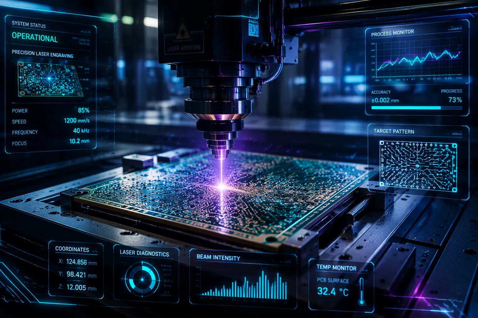
Demand for High-Precision PCB manufacturing grows fast in aerospace, medical, and 5G electronics. You might wonder how to bring laser production in-house for speed, accuracy, and flexibility. Focused laser beams shape and mark boards with micron-level precision. You load Gerber files straight into the laser system, removing outsourcing delays. This method cuts lead times and allows iterative design changes. You get full control over prototyping and production.
Key Takeaways
Making your own PCBs with a laser lets you test designs faster and keeps you in charge of your production timeline.
Laser drilling, cutting, and imaging achieve micron-level precision for tough applications.
A well-ventilated workspace and properly calibrated equipment keep you safe and produce steady quality.
Adding laser production to your workflow lets you test design changes quickly and cuts the cost of sending work to outside companies.
Benefits of In-House Laser Production for High-Precision PCBs
Core Laser Processes: Drilling, Cutting, and Imaging
Laser systems do three main jobs for making PCBs: drilling, cutting, and imaging. Each job uses a different laser. Each one gives special benefits for high-precision work.
Laser drilling makes microvias and through-holes with very high accuracy. UV lasers are great for this job. They make holes as small as 30 μm or less. The aspect ratio compares depth to diameter. It can go up to 15:1. This means you can drill deep, narrow holes without hurting the board's structure. Positional accuracy stays within ±15 μm. Registration accuracy reaches ±10 μm. Via positioning holds at ±15 μm. These tight limits meet the high needs of modern electronics.
Parameter | Tolerance / Value |
|---|---|
Hole diameter | Down to 30 μm or less |
Aspect ratio (depth to diameter) | Up to 15:1 |
Positional accuracy | ±15 μm or better |
Registration accuracy | ±10 μm |
Via positioning | ±15 μm |
Laser cutting shapes the board's outline and inside features. CO2 lasers cut nonmetal materials like fiberglass and composites. The beam turns material into vapor along the cut path. You get clean edges with very little heat damage. This process keeps the board's strength.
Laser imaging removes copper to make circuit traces. This process is called laser engraving. It has a big advantage over chemical etching. Chemical etching uses acids to remove unwanted copper. This method can create undercuts. The acid eats away material under the resist. Laser engraving makes vertical walls with no undercut. The trace edges stay sharp and clear. However, there is a trade-off. DIY laser engraving usually makes trace widths around 0.2 mm. Professional chemical etching can reach 0.10 mm or smaller. The better edge quality of laser engraving makes up for the slightly wider traces in many high-precision PCB uses.
Advantages Over Traditional Methods
Bringing laser production in-house changes how you work. You get speed, flexibility, and control.
Rapid prototyping happens within hours. You load Gerber files right into the laser system. The system reads the design and starts working right away. No waiting for outside suppliers. No shipping delays. You can test a new design, find problems, and fix it the same day.
Iterative design becomes easy. Each design change costs time and money with traditional outsourcing. You pay for new tooling and wait for new boards. In-house laser production removes these problems. You make changes in your design software. You export the new Gerber files. You run the laser again. This freedom lets you try new ideas and improve your work.
You keep full control over production. You decide the schedule. You adjust settings for each board. You check quality at every step. This control cuts lead times and makes better results. You also save money by reducing outsourcing costs.
In-house laser production gives real benefits for high-precision PCB manufacturing. The core processes of drilling, cutting, and imaging give you the tools you need. The advantages over traditional methods help you work faster and smarter.
Essential Equipment and Workspace Setup
Selecting the Right Laser System
You need to pick the right laser system for your PCB materials and jobs. Two main types handle PCB work: CO2 lasers and UV lasers. Each one has different strengths for your tasks.
CO2 lasers work well on nonmetal materials like fiberglass and composites. They cut and drill these materials with clean edges. UV lasers shine at fine detail work. They make ultra-fine microvias and small features.
The table below shows key performance numbers for each laser type.
Performance Metric | CO2 Laser | UV Laser |
|---|---|---|
Minimum Hole Diameter | 75 µm (3 mils) | 25 µm (1 mil) |
Drilling Speed | 500–2,000 pulses/sec | 5,000–30,000 pulses/sec |
Hole Quality | Clean, slight taper | Very clean, minimal taper |
Typical Use | Blind microvias | Ultra-fine microvias |
UV lasers hit a positional accuracy of ±10 microns. They also give a diameter accuracy of ±15 microns. These numbers matter for high-density PCB work. Match your laser choice to your most common board designs. Thin, fine-feature boards work best with a UV laser. Thicker boards with larger features may work well with a CO2 system.
Workspace Preparation and Safety Measures
Your workspace needs proper ventilation and safety systems. Laser cutting of fiberglass-based materials creates harmful fumes. You must control these fumes to protect your team.
Fiberglass and resin composites emit hazardous particulates that require specialized filtration. OSHA requires adequate ventilation systems to manage fumes and vapors generated during laser cutting operations.
You need a local exhaust ventilation (LEV) system placed close to the cutting area. This system should include:
High-efficiency particulate air (HEPA) filters to trap fine particles
Activated carbon filters to soak up chemical fumes
A design that keeps negative pressure in the cutting area
Regular upkeep and replacement of filters
Periodic air quality checks to confirm it works
One example of a good system is the PA-D800i. It has a rated air flow of 800 m³/h. The main filter is H14 HEPA, which traps 99.997% of particles at 0.3 µm. It includes an activated carbon filter to absorb smells and toxic gas. A flame retardant PTFE cartridge pre-filter adds safety. The system runs at less than 63 dBA.
You also need to calibrate your laser system often. Calibration keeps accuracy for each High-Precision PCB job. Check focus, alignment, and power output before each production run. This habit keeps your results steady.
Step-by-Step Implementation Process
Calibration, Parameter Optimization, and Material Testing
First, you load your Gerber files straight into the laser system. The software reads the design data and gets the machine ready. This direct loading stops translation errors and makes your whole workflow faster. You can move from design to production in just a few minutes.
Calibration comes first. You check the laser's focus, alignment, and power output before each production run. A well-calibrated laser gives steady results on all your boards. You check the beam position against a reference mark on the work surface. You confirm the focus distance matches your material thickness. You run a test pattern to check accuracy.
Parameter optimization follows calibration. You adjust power, speed, and focus for each material type. The table below shows starting values for drilling microvias in FR4 fiberglass.
Parameter | Recommended Value |
|---|---|
Laser Type | CO2 (10.6 μm) or UV (355 nm) |
Power | 10-20 W (CO2) |
Pulse Duration | Microseconds to nanoseconds |
Repetition Rate | 20-50 kHz |
Focus Spot Size | 20-50 μm |
You use trepanning for larger holes. This method moves the laser in a circle to lower taper and improve wall quality. You also make sure debris is removed during drilling. Built-up residue can hurt conductivity and ruin your boards.
Focus adjustment affects kerf width in cutting tasks. A well-focused laser gives a narrower kerf. A poorly focused one makes a wider cut. You do a focus test before your kerf test to ensure good calibration.
Higher pulse energy increases focus tolerance. This lets you focus the laser at a point midway through the PCB. You do not need to shift focus during cutting. This method reduces kerf width and gives a cleaner edge. Cross-section images show a narrower and more even kerf compared to normal lower-pulse-energy lasers.
Material testing finishes your preparation phase. You cut test patterns on sample boards. You measure hole diameters and edge quality. You check for heat damage and debris. You change your parameters based on these results. This testing phase stops costly mistakes during actual production runs.
Integrating Laser Production into Your Workflow
You fit the laser system into your design-to-production handoff. Your design team exports Gerber files from their CAD software. They save these files to a shared network folder. The laser operator imports the files directly into the machine's control software. This smooth handoff removes manual data entry and cuts down errors.
You set quality checkpoints throughout your production process. You inspect each board after drilling and cutting. You check hole positions against your design files. You measure trace widths after laser imaging. You write down every result for traceability. This record helps you see trends and catch problems early.
You create standard operating procedures for your team. These procedures cover machine startup, calibration checks, and maintenance schedules. You train each operator on proper laser safety and material handling. You cross-train multiple team members so production never stops when someone is away.
You schedule regular maintenance to keep your system running at its best. You clean lenses and mirrors every day. You check beam alignment each week. You replace filters per the maker's guidelines. You track maintenance activities in a logbook.
You watch production metrics to see how well you are doing. You track cycle times for each board type. You record yield rates and defect counts. You compare these numbers against your previous outsourcing results. This data shows the real impact of your in-house laser production.
Your workflow integration also includes design feedback loops. Your engineers see production results quickly. They spot design issues that affect making the boards. They make changes and test again the same day. This fast cycle of changes improves your board designs and your final products. You get the precision your High-Precision PCB applications need while keeping full control over your production schedule.
Overcoming Challenges for High-Precision PCB Results
Common Technical Issues and Solutions
Thermal damage ranks as the first challenge you will face. Mechanical cutting generates friction that burns edges and creates heat-affected zones. These zones compromise the dielectric properties of FR-4. Laser cutting solves this problem through precise heat regulation. UV lasers operate with minimal thermal impact, preventing damage to heat-sensitive materials. This reduces the risk of component delamination or discoloration.
Laser Type | Typical HAZ | Key Thermal Characteristic |
|---|---|---|
CO2 (10.6 μm) | 50-100 μm | Higher thermal spread, risk of charring |
Fiber (1.06 μm) | 10-30 μm | Moderate thermal impact |
UV (355 nm) | <10 μm | Minimal thermal damage |
Short-pulse lasers can reduce the heat-affected zone further by delivering energy in extremely brief bursts. This minimizes heat transfer to surrounding areas.
Advanced laser systems, particularly UV lasers, operate with minimal thermal impact, preventing damage to heat-sensitive materials. This directly addresses the most common thermal damage issues in high-precision PCB cutting.
Misalignment creates the second major hurdle. Panels can drift during drilling, causing microvias to miss their target pads. You can prevent this by tightly clamping panels and using thin support films. These films keep each board flat, avoiding tenting effects that cause stack misalignment.
Equipment Type | Graphic Alignment Accuracy | Interlayer Alignment Accuracy |
|---|---|---|
Conventional exposure machine | 25 μm | >50 μm |
High-precision alignment machine | ~15 μm | ≤30 μm |
Upgrading to high-precision alignment equipment reduces interlayer misalignment significantly. Advanced imaging systems also ensure precise positioning of the drill relative to the target pad.
Debris management directly determines your yield rates. Carbonized fragments and copper oxides block electroless copper nucleation, causing plating voids and weak adhesion. Redeposited material on sidewalls leads to CAF growth and intermittent opens. Plasma cleaning with O₂ or O₂+CF₄ removes carbonized polyimide fragments effectively. Chemical desmear handles copper oxides. Ultrasonic aqueous cleaning addresses redeposited material. Incomplete cleaning represents the highest yield-loss mode in high-volume production lines.
Building Operator Skills and Maintaining Quality
Your operators need structured training programs. They must understand laser safety protocols, material handling procedures, and machine calibration techniques. Cross-train multiple team members so production continues when someone is absent.
You maintain consistent quality through periodic calibration and process monitoring. Check focus, alignment, and power output before each production run. Track cycle times, yield rates, and defect counts. Compare these numbers against your outsourcing results. This data reveals trends and catches problems early.
Create standard operating procedures covering machine startup, calibration checks, and maintenance schedules. Clean lenses and mirrors daily. Check beam alignment weekly. Replace filters according to manufacturer guidelines. Document every maintenance activity in a logbook.
Your design feedback loop completes the quality system. Engineers see production results quickly and spot design issues affecting manufacturability. They make changes and test again the same day. This fast cycle improves board designs and final products. You achieve the precision your High-Precision PCB applications demand while maintaining full control over your production schedule.
In-house laser production transforms your High-Precision PCB manufacturing. You gain faster prototyping, tighter tolerances, and design flexibility. You reduce outsourcing costs and control your schedule completely.
The path forward is clear. Select the right laser system. Prepare your workspace with proper ventilation. Calibrate your machine. Optimize parameters. Test materials. Integrate the workflow. Maintain quality through monitoring.
Future advancements will expand your capabilities:
Ultra-fast femtosecond lasers drill near-zero heat-affected zones for ultra-thin substrates
AI integration enables real-time process control for consistent accuracy
Advanced laser systems process flexible circuits and ceramic substrates
Fiber laser technology reduces material waste and accelerates production
Evaluate your current bottlenecks today. Consult a supplier or request a demo. Take the next step toward precision and independence.
FAQ
What minimum hole diameter can a laser drill for a High-Precision PCB?
A UV laser drills holes as small as 25 µm. A CO2 laser reaches 75 µm. Your choice depends on the precision you need for your boards.
Do I need special software to run a laser PCB system?
No. You load Gerber files directly into the laser control software. This removes translation errors and speeds up your workflow from design to production.
How do I manage smoke and fumes from laser cutting?
You need a local exhaust ventilation system with HEPA and carbon filters. This protects your team and meets OSHA requirements for safe operation.
Can I cut thick boards with a CO2 laser?
Yes. CO2 lasers cut nonmetal materials like fiberglass. The maximum thickness depends on your laser power and the specific material you use.
See Also
Comprehensive PCBA Manufacturing Process Guide for Novices and Pros
Essential Raw Materials Required for PCBA Assembly Production
Crucial Actions to Enhance PCBA Durability for Extended Operation
Technique for Applying Double-Sided Reflow Soldering in PCBA Manufacturing
