Advanced Solder Joint Cross-Section Analysis Techniques for 2026
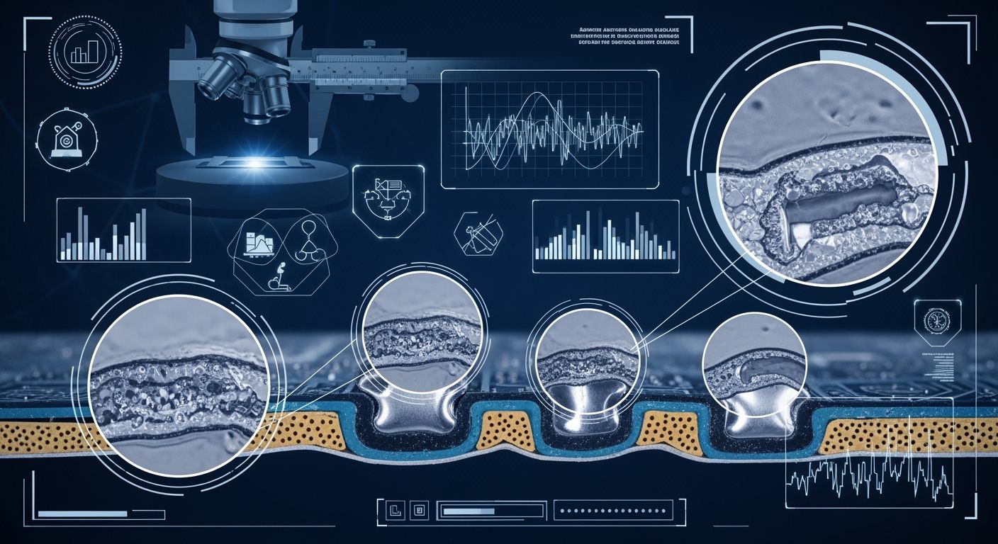
Engineers use advanced solder joint cross-section analysis to check electronic assemblies. These methods help improve quality and reliability. Modern analysis lets engineers look from different angles. It also measures things at the micron level. The table below shows important differences:
Feature | Traditional Methods | Advanced Techniques |
|---|---|---|
Viewing Angle | Top-down only | Multi-angle observation |
Defect Detection | Limited to visible defects | Detects hidden defects |
Inspection Technology | Conventional microscopes | 3D digital microscope systems |
Depth of Field | Standard depth | Extended Depth of Field (EDF) |
Structural Detail Visibility | Often blocked by components | Reveals hidden structural details |
Measurement Precision | Basic measurement | Micron-level measurement |
Cross-section analysis finds hidden solder defects. It helps make sure manufacturing is high-quality.
Key Takeaways
Advanced solder joint analysis helps products last longer. It finds hidden problems like cracks and voids.
New methods, like 3D X-ray tomography and AI image analysis, make checking faster and more correct.
Cross-section analysis is important for quality control in big industries. These include automotive and aerospace. It helps keep things safe and strong.
Engineers use special software and machines to make the analysis easier. This also lowers mistakes made by people.
Predictive analytics and smart manufacturing help spot problems early. This leads to better product designs and fewer failures.
Why Solder Joint Cross-Section Analysis Matters
Reliability and Quality Control
Cross-section analysis is very important for keeping electronics safe. Engineers use it to check solder joints and make sure they last a long time. They look for cracks and voids in solder joints. They also find intermetallic compounds that can hurt the joint. These checks help companies keep their products high-quality. They stop hidden problems from making products fail.
Note: Cross-section analysis is the best way to check hidden solder joints in BGAs and CSPs.
The table below shows how these methods help with reliability and quality:
Evidence Type | Description |
|---|---|
Internal Defect Detection | X-ray imaging finds bubbles, voids, and not enough filling without breaking the part. |
Detailed Interface Analysis | Section analysis gives details about the interface and intermetallic compounds using microscopes. |
Quality Assessment for Hidden Joints | These methods are the only good way to check hidden solder joints like BGAs and CSPs. |
Manufacturers use cross-section analysis to count layers and measure thickness. They check plating quality and find defects from making the product. They also follow IPC rules to make products stronger.
Failure Analysis and Defect Detection
Failure analysis uses cross-section checks to find out why electronics stop working. Engineers look at solder joints to spot plating voids, delamination, cracks, and resin smearing. These problems can cause electrical failures and mess up signals.
Plating voids make electrical connections weak.
Delamination messes up signals.
Cracks happen from stress or heat.
Solder joint problems cause bad connections.
Resin smearing makes conductivity worse.
About 70% of electronic failures come from packaging structure problems. The Engelmaier fatigue model guesses how long solder joints last using strain and ductility. The type-I interval censored data method predicts how long lead-free solder joints last in heat tests. These models help check quality and make PCB manufacturing better.
Advanced Techniques Overview
Ion Beam Polishing & SEM
Ion beam polishing and SEM are important tools for cross-section analysis. Engineers use ion milling to get samples ready without hurting them. This keeps the inside parts of the solder joint safe. SEM gives clear pictures that show interfaces, voids, and defects. The process mixes sample prep and imaging, making it easier and more reliable.
Advantage | Description |
|---|---|
Damage-free preparation | Ion milling stops stress and keeps inside parts safe. |
Enhanced clarity | Clear pictures show interfaces, voids, and defects well. |
Workflow efficiency | The process is smooth and helps get the same results every time. |
These methods help engineers check cross-sections and materials more accurately. They can find hidden defects and do better failure analysis. Ion beam polishing and SEM help makers check solder joint quality and reliability.
3D X-ray Tomography
3D X-ray tomography lets engineers check solder joints without breaking them. They use it to see hidden spots inside tricky packages like BGAs. The method makes 3D pictures that show inside defects like voids and cracks. It helps with cross-section analysis by showing everything without cutting the sample.
X-ray checks find bubbles and voids in solder joints.
3D pictures let engineers see the structure from different sides.
The process helps find defects and supports failure analysis.
CT makes finding problems easier than old methods. Engineers spot issues faster and make better choices about product quality. 3D X-ray tomography helps check materials and makes products more reliable.
AI Image Analysis
AI has changed how engineers look at solder joints. Most CNN models help find defects in solder joints. AI image analysis uses machine learning to sort features faster than doing it by hand.
Using machine learning for image analysis is much faster and more accurate than doing it by hand. ML-algorithms can handle lots of image data, like the kind from X-ray tomography, quickly. Algorithms do not make mistakes from human error like people do.
AI works through lots of image data fast. It cuts down mistakes and makes results more steady. Engineers use AI for cross-section checks and failure analysis. The technology helps makers find defects and make solder joints stronger.
Metallography Methods
Metallography methods are better now with CT. CT gives a 3D look at solder joint structures. Engineers use these methods to find inside defects like voids and cracks. Old metallography needed many sections, but CT makes things more exact and faster.
New metallography helps check materials and cross-sections. Engineers can look at solder joint quality in more detail. These methods help makers spot problems early and stop failures.
Solder Joint Analysis Workflow
Sample Preparation Tools
Engineers use special tools to get samples ready. They pick equipment that gives accurate and steady results. The table below shows the best tools for cross-section preparation in 2026:
Tool Name | Description |
|---|---|
Buehler AutoMet 250 | A precision grinder and polisher for metallographic sample preparation. |
Buehler EcoMet 30 | A semi-automatic grinder and polisher designed for efficient sample preparation. |
Buehler VibroMet 2 | A vibratory polisher that provides uniform polishing for metallographic samples. |
Buehler IsoMet 1000 | A precision cutter for accurate cross-sectioning of samples. |
Buehler IsoMet High Speed Pro | A high-speed precision cutter designed for rapid sample preparation. |
Leica EM TXP | A tool for advanced sample preparation in electron microscopy. |
Optical microscopy and scanning electron microscopy help engineers study solder joints closely. These tools let engineers check cross-sections after tests.
Integrated Software
Software makes the analysis process easier. Engineers use it to take pictures and measure cross-sections fast. Many systems find defects and measure layers automatically. Engineers compare results and watch quality changes over time. The software keeps data safe and makes reports. It also helps teams work together.
Tip: Integrated software helps avoid mistakes and makes cross-section analysis faster.
Automation & Data Management
Automation and data management help engineers work faster. Engineers use learning methods to guess layer thickness from pyrometer signals. This way, they do not need to process data by hand. Temporal sampling algorithms handle different scan lengths, so models can be trained easily. Real-time monitoring finds small layer-thickness changes, even as tiny as 20 µm. These features help with advanced monitoring and quality control.
Automation makes analysis quicker and more correct.
Data management systems keep results safe and organized.
Real-time monitoring lets engineers spot defects early.
Engineers get faster and more reliable cross-section analysis with automated workflows and strong data management.
Comparing Methods
Precision & Accuracy
Engineers look at different methods to find the best one. Each method has its own special strengths for cross-section analysis. Mechanical cross-section analysis can show features as small as 10 microns. Atomic force microscopy shows tiny surface details. Electron backscatter diffraction and transmission electron microscopy give pictures at the atomic level. Energy-dispersive X-ray spectroscopy and X-ray microanalysis help find materials and contamination. Scanning electron microscopy gives clear images. X-ray computed tomography lets engineers see inside joints without cutting them.
Method | Precision and Accuracy Benefits |
|---|---|
Mechanical Cross-Section Analysis | Can analyze features as small as 10 microns with few polishing marks. |
Atomic Force Microscopy (AFM) | Shows nanoscale surface shapes and roughness for fine features. |
Electron Backscatter Diffraction (EBSD) | Gives very clear pictures and atomic-level analysis with more thinning. |
Energy-Dispersive X-ray Spectroscopy (EDS) | Helps with elemental analysis at certain spots, finding materials and contamination. |
Scanning Electron Microscopy (SEM) | Gives clear pictures for detailed shape analysis and surface study. |
Transmission Electron Microscopy (TEM) | Gives very clear pictures for atomic-level analysis. |
X-ray Microanalysis (WDS) | Gives more exact elemental analysis with better spectral detail than EDS. |
Makes 3D pictures without breaking samples to find inside defects before cutting. |
Speed & Throughput
Modern tools help engineers work faster. Automated systems can handle many samples at the same time. AI image analysis finds defects quickly. 3D X-ray tomography lets teams check lots of solder joints without breaking them. These upgrades help engineers finish failure analysis fast. They can check more products in less time.
Tip: Automation and software help stop mistakes and make work faster.
Reliability Gains
Advanced methods make products stronger. Picking the right materials makes joints tougher and helps them handle heat. New designs spread stress so joints do not break. Better ways to make things control temperature and improve solder joint quality. Protective coatings keep joints safe from water and dirt.
Aspect of Reliability | Contribution of Advanced Techniques |
|---|---|
Material Selection | Stronger joints and better heat resistance by picking the right alloys and additives. |
Structural Design | New designs spread stress so joints do not fail. |
Manufacturing Process | Careful temperature control and advanced soldering make joints better. |
Environmental Protection | Protective coatings keep joints safe from water and dirt. |
These improvements help companies make stronger products. Engineers can trust results from advanced cross-section analysis.
Practical Applications
Automotive Electronics
Automotive engineers use advanced analysis to keep electronics safe. They check printed circuit boards for hidden defects. This helps them make sure the boards work well. It also helps them guess how long the boards will last in tough places. Manufacturers change their processes to waste less and make more good products. Checks make sure products follow industry rules. The table below shows how analysis helps automotive electronics:
Application Type | Description |
|---|---|
Quality Control | Makes sure PCBs are strong and finds hidden defects. |
Failure Analysis | Helps find why solder joints and PCBs fail. |
Compliance Assurance | Checks if products follow industry rules for automotive electronics. |
Process Improvement | Changes manufacturing to make more good products and waste less. |
Long-term Performance | Guesses reliability when things get hot or wet. |
Aerospace & Defense
Aerospace and defense teams use cross-section analysis to find defects and make products stronger. Mechanical testing checks how strong things are under stress. Thermal testing shows what happens when temperatures change and finds aging problems. Environmental testing checks for moisture and finds delamination. Engineers use X-ray inspection to see inside solder joints. Optical methods cannot see these hidden parts. Without X-ray checks, defects like voids and non-wetting can cause early failures.
Testing Method | Purpose | Benefits |
|---|---|---|
Mechanical Testing | Checks strength under stress | Finds early fatigue and cracks |
Thermal Testing | Shows temperature changes | Finds aging from heat |
Environmental Testing | Checks moisture exposure | Finds delamination problems |
Optical inspection cannot find hidden defects in bottom-terminated parts.
X-ray inspection shows inside solder joints that are invisible.
High-Density PCB Case Study
A big electronics company had many failures in high-density PCBs for industrial controls. Engineers used cross-section analysis on solder joints. They found voids and cracks that normal checks missed. They made soldering better and added real-time monitoring. These changes made products stronger and cut warranty claims. This case shows how analysis helps companies keep quality and protect complex assemblies.
Engineers who use advanced analysis can find hidden defects and make products work better. These methods help with quality control and keep electronic systems safe.
Future Trends
Predictive Analytics
Predictive analytics is changing how engineers check solder joints. Engineers use data from microscopes to find problems early. Optical microscopy helps them take pictures and find failures. FTIR-microscopy shows where contamination comes from, like flux. Metallographic microscopy and SEM-EDS help engineers learn why things fail. Engineers use these tools together to make models that guess how solder joints will work. They can fix problems before they happen and make products better.
Engineers use optical microscopy to record samples.
FTIR-microscopy finds where contamination starts.
Metallographic microscopy and SEM-EDS help find why things fail.
Cross sectioning shows inside parts for making predictions.
Smart Manufacturing Integration
Smart manufacturing now works with solder joint analysis. This helps make products stronger. Engineers use cross-sectional analysis to check bump metallurgy and construction. They look for voids in solder joints, which can make them weaker. Lead-free solder materials are tested for their makeup and contamination. Automated systems collect data and change processes right away. This helps manufacturers make better products and stop defects.
Study Focus | Key Findings |
|---|---|
Solder Joint Characteristics | Cross-sectional analysis checks bump metallurgy and construction for reliability. |
Voids in Solder Joints | Voids make solder joints last less and become weaker. |
Lead-Free Solder Materials | Cross-sectional analysis checks metallurgical makeup and Pb contamination effects. |
Green Analysis Techniques
Green analysis techniques help engineers protect the environment. They check solder joints while keeping things safe. Appearance inspection finds visible defects. X-ray fluoroscopy finds inside problems without breaking the joint. Soldering strength tests check how strong joints are. Reliability verification checks how joints work in tough conditions. Cross-section analysis shows microstructure and alloy layer growth. Dyeing tests show if solder joints are good. Elemental analysis checks what solder is made of. Tin whisker observation looks for tiny growths that cause failures. Reliability aging tests copy long-term use. Both non-destructive and destructive tests help check quality.
Method | Purpose |
|---|---|
Appearance Inspection | Find visible defects in solder joints. |
X-ray Fluoroscopy | Find inside problems without breaking the solder joint. |
Soldering Strength Test | Check how strong solder joints are. |
Reliability Verification | See how joints work in tough conditions. |
Cross-section Analysis | Show inside microstructure and alloy layer growth. |
Dyeing Test | Check solder joint quality with dye. |
Elemental Analysis | Find out what solder is made of. |
Tin Whisker Observation | Look for tin whiskers that cause failures. |
Reliability Aging Tests | Copy long-term use to check durability. |
Non-destructive Testing | Includes appearance inspection and X-ray fluoroscopy. |
Destructive Analysis | Includes cross-section analysis and other tests to check solder joint quality. |
Engineers use green techniques to keep products safe and help the environment.
Advanced solder joint analysis gives engineers better ways to check reliability and quality. The table below shows how new methods help make electronics stronger:
Technique | Benefit |
|---|---|
Optimizing solder composition | Makes joints work better and lowers defects. |
Controlling reflow profile | Stops early failure when stressed. |
Implementing design features | Makes products more reliable. |
Engineers use X-ray inspection, cross-sectioning, and thermal cycling tests to find problems and stop failures. They need to look at these methods to meet future needs in solder technology.
X-ray inspection finds voids.
Cross-sectioning checks microstructure.
Electrical testing makes sure things work.
FAQ
What is the main benefit of advanced solder joint cross-section analysis?
Engineers can see hidden defects better. They make products more reliable and control quality. Advanced methods show cracks, voids, and intermetallic compounds that old inspections miss.
Which industries use these techniques most often?
Industry | Application |
|---|---|
Automotive | Safety and durability |
Aerospace | High-reliability systems |
Consumer Electronics |
How does AI image analysis help engineers?
AI image analysis finds defects faster. It lowers mistakes made by people. Engineers use machine learning to sort features and look at big image sets quickly.
Can 3D X-ray tomography replace destructive testing?
3D X-ray tomography lets engineers see inside without breaking things. Engineers still use destructive testing to check microstructure in detail. Both methods work well together.
What tools do engineers need for sample preparation?
Precision cutters
Automated grinders and polishers
Electron microscopy preparation tools
These tools help engineers get accurate and steady results.
See Also
Understanding Solder Paste Types and Components in SMT Assembly
Essential Tips for Effective Wave Soldering in SMT
Exploring Welded End Designs for SMC and SMD Components
