8 Typical Defects of BGA
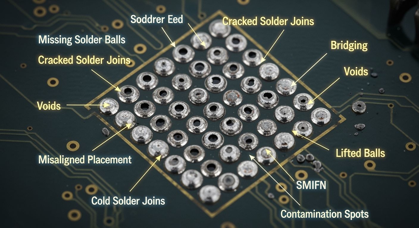
You often see eight main typical defects when working with BGA packages. These are cold solder joints, head-in-pillow, solder joint voiding, solder bridging, non-wet open, misalignment, tombstoning, and solder balling. Each typical defect can hurt how well the assembly works. The table below shows how often some defects happen in BGA packages:
Defect Type | Prevalence Rate |
|---|---|
Bridging | Minimal |
Misregistration | Occasional |
Missing Solder Balls | Not reported |
Voids | Rarely severe |
Internal Shorts | 30% failures in one case |
Overall Defect Rate | 1 to 4 ppm |
You need to know about these typical defects in BGA packages. This helps you keep electronic assemblies working well. It also helps you avoid common problems and lower failure rates. Checking BGA packages is very important. Warpage, tight spaces, and other problems make normal checks harder. Warpage often causes these typical defects, especially in BGA packages. So, you should check for warpage at every step.
Key Takeaways
Learn about the eight common defects in BGA packages. This helps make assembly more reliable.
Check often for cold solder joints and head-in-pillow defects. This stops devices from failing.
Watch your reflow process to keep away problems like tombstoning and solder bridging.
Use X-ray inspection to find hidden defects. It also checks if solder joints are lined up right.
Use good process controls and training. This lowers defects and makes products better.
Cold Solder Joints in BGA
Symptoms
You can find cold solder joints in BGA assemblies by looking for some signs.
The surface may look dull, rough, or chalky.
The solder might look like a ball and not blend with the pad.
You might see cracks or spaces between the solder and the lead.
You can also check for electrical problems.
Put your multimeter on resistance mode.
A good joint will show almost no resistance.
If the number changes when you press or move the part, it is a cold solder joint.
Causes
Cold solder joints usually happen because of mistakes when soldering.
Here is a table that lists the main causes and what they mean:
Cause of Cold Solder Joints | Description |
|---|---|
Insufficient peak temperature during reflow | The heat does not get high enough (less than 217°C for SAC305 solder). |
Rapid cooling rates | The solder does not form strong bonds, so the joint is weak. |
Contaminated pads or leads | Dirt, old flux, or water stops the solder from sticking well. |
Inadequate dwell time above liquidus temp | Not enough time at the right heat keeps the solder from flowing and bonding right. |
Impact
Cold solder joints are a common problem in BGA packages. You might see connections that work sometimes or not at all. These problems can make devices stop working or break while being used. If you do not fix cold solder joints, your assembly may not last long and repairs will cost more. You should check for these defects to keep your BGA assemblies working well.
Head-in-Pillow Defect
Symptoms
You might see head-in-pillow defect when you check BGA assemblies. If you use an angled X-ray, look for a shape like a snowman. This means the BGA ball does not join with the solder paste. You will see two round shapes with a line between them. They do not blend into one shape. This gap can make circuits work sometimes and fail other times. These defects are hard to find without special tools. Head-in-pillow is one of the most common BGA defects.
Causes
Many things can cause head-in-pillow defects. You need to watch both your process and the materials you use. The table below lists the main causes and what they mean:
Contributing Factor | Description |
|---|---|
Poor wetting | Solder does not flow well because of oxidation or weak flux. |
Warpage | The PCB or package bends during reflow, which affects the solder joint. |
Low flux activity | The flux in the paste is not strong enough to help the solder bond. |
Material interactions | The solder paste and BGA ball alloy do not work well together. |
Component placement accuracy | The BGA is not placed correctly, so the joint does not form as it should. |
PCB design factors | The design makes it hard for solder to wet, or pads are not flat enough. |
Impact
Head-in-pillow defect can cause big problems in BGA assemblies. The table below shows the main impacts you should know:
Impact Type | Description |
|---|---|
Mechanical Weakening | The solder joint becomes weak and can break under stress. |
Intermittent Electrical Failures | The connection may work sometimes but fail during use, leading to unreliable products. |
Reduced Product Reliability | The overall reliability drops, and you may see more failures in the field. |
Weak Interface | The joint may keep electrical contact but lacks strength, making it risky for long-term use. |
Detection Difficulty | You often need special tests to find this defect, so it can hide in your assemblies. |
You should always check for head-in-pillow defect. It can make your BGA products less reliable and lower their quality.
Solder Joint Voiding
Symptoms
You can spot solder joint voiding in BGA assemblies by looking for signs that affect performance. Devices may show unstable connections or fail during testing. Sometimes, you notice random resets or signal drops. If you use X-ray inspection, you see dark spots inside the solder joints. These spots mean there are gaps or holes where the solder did not fill completely. X-ray imaging helps you check many joints at once without damaging the board. You can find voids as small as 5% of the joint area. This makes X-ray inspection a reliable way to detect common defects in BGA packages.
Causes
Many factors cause solder joint voiding. You need to control your process to avoid these defects.
Keep your workspace clean and follow the right steps to lower the risk of voids.
Here are the main causes:
Solder paste handling: Store and handle paste correctly to prevent voids.
Reflow time and ramp rate: Follow the right heating profile to let gases escape.
Component manufacturing: Defects in parts can lead to voids.
Circuit board and component contamination: Clean parts help avoid trapped gases.
You also need to watch for these conditions:
Solder paste chemistry and flux volatiles: High volatile content can trap gases in the solder.
Improper reflow thermal profile: Short soak times and not enough heat keep gases from escaping.
Impact
Solder joint voiding affects the strength and reliability of BGA assemblies. You may see weak joints that break under stress. Devices can fail early or work only sometimes. Voids lower the electrical and mechanical performance of the solder joint. If you ignore these defects, your products may not last long. You should always check for solder joint voiding to keep your assemblies strong and reliable.
Solder Bridging in BGA Packages
Symptoms
You can find solder bridging in BGA assemblies by looking for some signs.
You might see metal connecting pads that should not touch.
Extra solder can make a bridge and let electricity go the wrong way.
Devices might not pass tests or show short circuits when checked.
Sometimes, two or more balls look stuck together in X-ray or under a microscope.
If you notice these signs, check for other problems nearby too.
Causes
Many mistakes in the process can cause solder bridging in BGA packages. The table below lists the main groups and details:
Category | Specific Factors |
|---|---|
PCB Related | Pad size and spacing, missing solder mask, solder mask misalignment, solder mask thickness |
Component Related | Moisture sensitivity, substrate warpage, ball coplanarity error |
Solder Paste Printing Related | 1:1 aperture size, contaminated stencil, excess paste, paste slumping, poor board support, misalignment |
Placement Related | Too much placement pressure, poor board support, placement misalignment |
Reflow Related | PCB or component warpage, too much flux, heavy components pressing down on molten solder |
Solder bridging often happens if you use too much solder paste or if pads are too close. Stencils that are not lined up right and high heat during reflow also make it worse.
Impact
Solder bridging can make big problems in BGA circuits. Short circuits can form and stop your device from working. You might also see bad wetting, which makes the joint weak. These problems can make your assembly less reliable over time. Voids can trap air and lower how well heat and electricity move. If the reflow heat is not even, the BGA can bend. This bending can make some solder balls melt first and cause bridges that hurt how the circuit works.
Always check your process and look at assemblies to find solder bridging early. This helps you avoid expensive fixes and keeps your products working well.
Non-Wet Open (NWO) Defect
Symptoms
You can find non-wet open defects in BGA assemblies if you know what to look for. These defects are hard to see with your eyes. Here are some signs you might notice:
The device works sometimes but fails other times.
Electricity stops flowing because of open circuits.
You might see cracks near the solder joints.
If you see these signs, check for non-wet issues in your BGA assembly.
Causes
Non-wet open defects happen when solder does not stick to the pad during reflow. You can stop many problems by controlling your process. The most common causes include:
Solder pads get oxidized and solder cannot bond well.
Solder pads do not get enough heat, especially in the center of big BGA packages or on pads with lots of copper.
The board bends from heating and makes gaps between solder balls and pads.
Always check your process and materials to lower the risk of non-wet defects.
Impact
Non-wet open defects can hurt the electrical connection and reliability of your BGA assemblies. You may not see these defects right away, but they can cause big problems later. Here are some impacts you should know:
Electrical connections are weak or missing, like the head-in-pillow effect.
Failures happen sometimes and are hard to find during testing.
Devices may have reliability issues, especially those that need high performance, like mobile phones.
If you do not fix non-wet open defects, your products may fail in the field. Always inspect your assemblies and use good process control to avoid these problems.
Ball Grid Array Misalignment
Symptoms
You can find ball grid array misalignment by checking for certain signs. Sometimes, solder balls are not lined up with the pads. This can make open circuits or short circuits. Devices may fail tests or act unstable. Some connections might not work at all. Sometimes, the device works only part of the time.
To help you spot misalignment, you can use different inspection methods. Here is a table that shows the best ways:
Method | Description |
|---|---|
Visual or Optical | Use magnifying tools to look for misalignment and other problems. |
Take gray pictures to check alignment and find misalignment without hurting the board. | |
Infrared Thermography | Use heat pictures to find problems caused by misaligned solder joints. |
Acoustic Microscopy | Use sound waves to find misalignment and other problems in solder joints. |
Tip: X-ray inspection is good for hidden solder joints in BGA packages.
Causes
You can stop many defects if you know what causes misalignment. Here are the main reasons:
Pads that are not the same size or not lined up can cause soldering problems.
Small pads hold less solder paste, so joint height is not even.
Heat changes can stretch or shrink joints and cause failures.
Bad placement means solder balls miss the right pads.
Good placement helps the BGA line up during reflow, but bad placement causes misalignment.
If you control these steps, you lower the chance of ball grid array misalignment.
Impact
Ball grid array misalignment can cause big problems in your assemblies. When misalignment happens, the board can bend. This bending leads to solder joint defects and connection failures. Devices may not work right, and you might see fewer good products. If you do not fix misalignment, you risk bad performance and more failures in the field.
Tombstoning in BGA
Symptoms
Tombstoning happens when one end of a part lifts up. It looks like a tiny gravestone under the BGA. One side rises, but the other side stays on the pad. You might see missing connections during tests. Devices may not turn on or show random errors. Sometimes, you need X-ray or special tools to find this problem. The defect hides under the package and is hard to see.
Tip: If a device works sometimes but fails other times, check for tombstoning under the BGA.
Causes
Tombstoning starts when solder joints do not have equal forces. Many things can cause this problem:
Pads with different sizes or shapes heat up unevenly.
Parts placed wrong can make solder pull unevenly.
Dirty or rusty materials make solder stick less.
If one pad melts first, it pulls the part up.
Pads that are not the same or copper areas that are different cause heat problems.
Too much or too little solder paste changes how solder sticks.
Copper layout or routing can slow heating on one side.
Small parts are more likely to move from surface tension.
Heating up too fast or not soaking enough can melt solder unevenly.
Changes in solder paste or small placement mistakes add risk.
Impact
Tombstoning can make big problems in BGA assemblies. You might get open circuits that stop electricity. Solder joints become weak and break easier. Devices may fail sometimes and work other times. The solder joint gets smaller, so it cannot cool well. Over time, you may see more problems, especially as devices shrink and use more power. If you do not find tombstoning early, your products may fail later.
Solder Balling Defect
Symptoms
You can find solder balling defects by looking for small, round solder balls. These balls are scattered around the BGA package. Some balls show up near the edges or between the pads. Sometimes, you see them stuck to the board or inside joints. Devices might not pass tests or show random errors. You may notice bad electrical connections or short circuits. X-ray inspection can help you find hidden solder balls under the BGA.
Tip: Always look for loose solder balls after reflow. They can cause problems later.
Causes
Many things in the process or materials can cause solder balling. You must control each step to lower the risk.
Solder ball damage happens with old sockets or parts that do not match. High heat and needlepoint sockets can change the shape of solder balls. Claw-type sockets can scratch the balls.
Solder ball falling happens when solder paste does not stick well. Dirt or nickel oxidation makes it worse. Too much gold plating can make solder balls break and fall off.
Solder ball oxidation is common if balls stay in air too long. This often happens during the second inspection step.
Bad stencil design or too much paste can make extra balls during printing.
Fast or uneven heating can make solder splash and form balls.
Impact
Solder balling defects can make your BGA assemblies less reliable. Loose solder balls can cause short circuits or open connections. Devices might fail early or work only sometimes. You may see random errors or weak performance. Solder balls can move and cause new problems after assembly. If you do not fix these defects, your products may fail later. Always check for solder balling and use good process control to keep your assemblies strong.
Typical Defects Summary Table
You need a simple way to compare common problems in bga assemblies. This summary table helps you see the main signs and causes for each defect. Use it when you check or fix your boards.
Defect Name | Main Symptoms | Common Causes |
|---|---|---|
Cold Solder Joint | Solder looks dull or rough, cracks, weak joints | Not enough heat, cooling too fast, dirty pads, short reflow |
Head-in-Pillow | Snowman shape on X-ray, open circuits | Warpage, poor wetting, weak flux, bad placement |
Solder Joint Voiding | Dark spots on X-ray, weak or unstable joints | Trapped gas, bad paste, poor reflow profile |
Solder Bridging | Short circuits, solder between pads | Too much paste, close pads, stencil errors |
Non-Wet Open (NWO) | Sometimes fails, open circuits | Oxidized pads, low heat, board warpage |
Misalignment | Balls not on pads, open or short circuits | Bad placement, uneven pads, thermal stress |
Tombstoning | One end up, missing connections | Uneven heating, pad size, bad placement |
Solder Balling | Loose solder balls, random shorts | Extra paste, fast heating, dirty surfaces |
Tip: Keep this table close when you work with bga packages. It helps you find problems faster and fix them before they get worse.
Preventing BGA Defects
Process Control Tips
You can prevent most bga assembly problems by controlling your process from start to finish. Start with clean boards and components. Always store your solder paste at the right temperature. Use fresh paste for every manufacturing run. Set your stencil printer to apply the right amount of solder. Check the stencil for damage or dirt before each use.
Set your pick-and-place machine to place each bga in the correct spot. Make sure the machine lines up the balls with the pads. Watch for board warpage before reflow. Use a flat support to keep the board steady.
Control your reflow oven settings. Use a thermal profile that matches your solder type. Heat the board slowly at first. Let the solder reach the right temperature and stay there long enough to melt and flow. Cool the board at a steady rate. This helps the solder form strong joints and reduces voids.
Tip: Review your reflow profile often. Small changes in temperature or time can cause big quality problems in bga assembly.
Inspection Best Practices
You need strong inspection steps to catch defects early in bga assembly. Use X-ray inspection to check for hidden problems. Look for these signs:
Ball shape: Make sure each solder ball collapses the same way after reflow.
Alignment: Check that every bga ball sits on its pad.
Voiding: Find gas pockets inside the solder joints.
Open joints: Spot any places where the solder did not connect.
Head-in-pillow: Detect joints that look joined but are not solid.
Solder bridging: Find extra solder between pads.
Solder volume: Check for too much or too little solder.
You can also use optical tools to check for misalignment and missing balls. In high-reliability manufacturing, combine X-ray with other tests for full quality control. Early detection keeps your bga assembly strong and lowers the risk of field failures.
You help keep your bga assemblies working well by finding and fixing problems early. Careful checks with X-ray and optical tools let you see hidden issues. Watching heat levels during reflow and teaching your team makes quality better.
Look for weak joints, misalignment, and missing solder balls.
Make sure your equipment is set up right for good results.
Train your team to notice problems before they cause failures.
If you manage defects early, your products will be stronger and you will have fewer unexpected problems.
FAQ
What is the most common BGA defect?
You often see cold solder joints and head-in-pillow defects. These problems happen because of poor soldering or warpage. You should check for these first when you inspect BGA assemblies.
How can you spot a solder bridge in a BGA?
You can use X-ray inspection to find solder bridges. Look for metal connecting two pads that should not touch. Devices may also fail tests or show short circuits.
Why does tombstoning happen in BGA packages?
Tombstoning happens when one side of a part heats faster than the other. Uneven heating or pad sizes can cause one end to lift up. You should control your reflow process to prevent this.
Can you fix BGA defects after assembly?
You can fix some defects, like cold solder joints, by reworking the board. Use special tools to remove and replace the BGA. Some defects, like hidden voids, may need advanced repair or full replacement.
What tools help you inspect BGA defects?
You can use X-ray machines, optical microscopes, and acoustic microscopes. X-ray is best for hidden joints. Optical tools help you check alignment and missing balls.
See Also
Tips for Preventing Frequent Errors in BGA Assembly
Ensuring Perfect BGA Assembly Through Effective Quality Management
Identifying and Preventing Typical Defects in SMT Assembly
Innovative Methods for Reliable BGA Assembly in Electronics
Seven Essential Quality Control Steps for Through Hole PCB Assembly
