X-Ray Inspection Technology for Detecting Hidden Defects in Multilayer PCB Assemblies
X-ray inspection lets engineers look inside printed circuit boards. It helps them find hidden defects that can hurt reliability. PCB x-ray inspection helps find solder problems in multilayer pcbs. LTPCBA uses pcb x-ray inspection to check quality in complex pcbs. X-ray inspection is more important as pcbs get more advanced.
Key Takeaways
X-ray inspection helps engineers look inside multilayer PCBs. It finds hidden problems like solder voids, blocked vias, and cracks. Other tests often miss these defects.
This method finds problems early and does not hurt the board. It helps make complex PCB assemblies more reliable and better in quality.
Using both x-ray inspection and automated optical inspection (AOI) checks quality well. X-ray finds inside defects. AOI checks the surface quickly. Together, they make sure nothing is missed.
X-Ray Inspection in PCB Manufacturing
How X-Ray Works
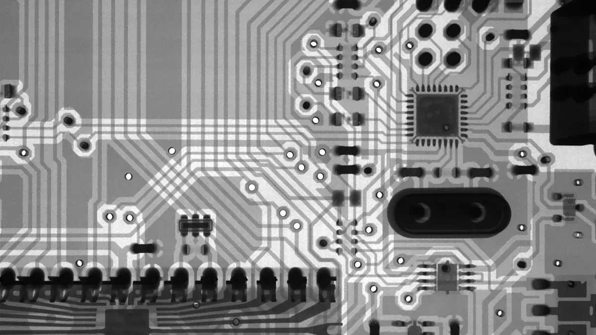
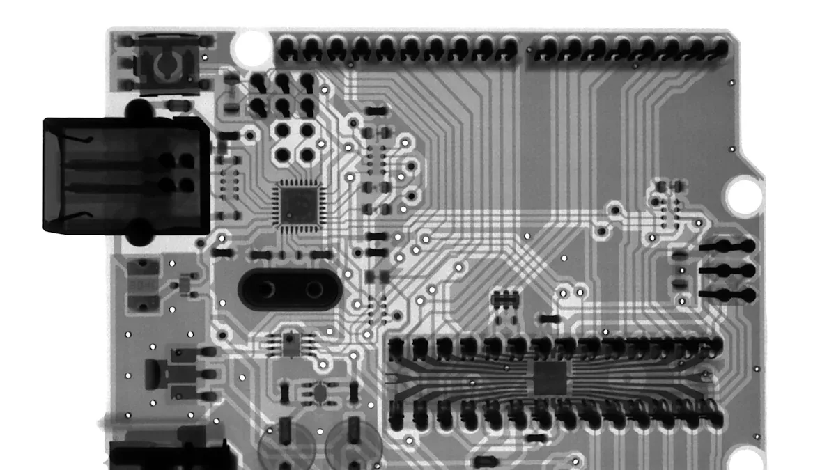
PCB x-ray inspection uses special tools to look inside circuit boards. It does not hurt the board. X-ray beams go through the PCB. Special detectors take pictures of the inside. Engineers use both 2D and 3D images. 2D imaging gives flat pictures of the board. 3D imaging, like CT, takes many 2D pictures from different sides. These pictures join together to make a 3D view of the PCB. This helps engineers see layers, connections, and very tiny parts as small as 1 micron.
X-ray imaging in PCB manufacturing uses projection-based systems. Divergent x-ray beams go through the board and make radiographs on flat-panel detectors.
3D x-ray microscopy (XRM) uses both geometric and optical magnification. This lets engineers see small details deep inside the PCB.
New detectors and scintillators help find small defects more easily.
LTPCBA uses advanced x-ray inspection systems to check quality. These systems help make sure every PCB meets strict rules.
Detecting Hidden Defects
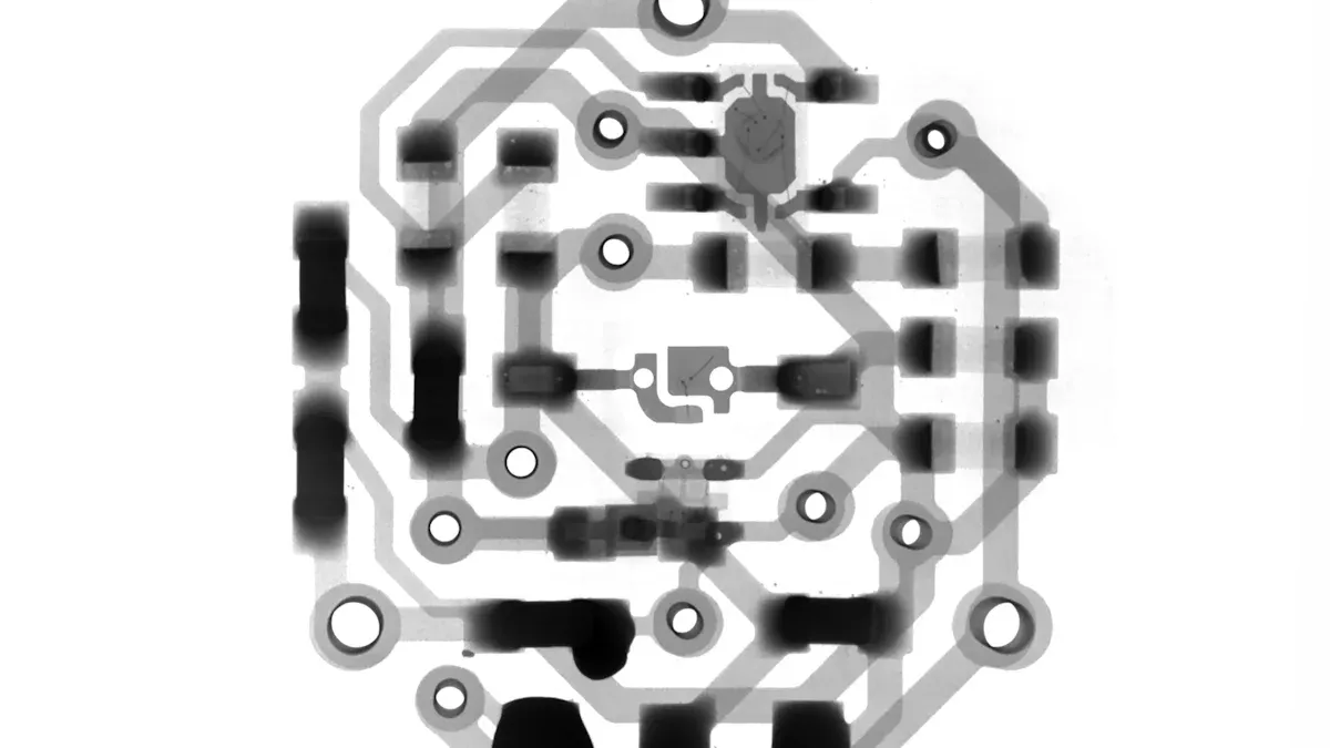
PCB x-ray inspection finds inside problems that other tests miss. X-rays go through the board and show things like solder voids, cracks, and parts that do not line up. In multi-layer PCBs, these problems can hide under parts or between layers. X-ray inspection finds them without taking the board apart.
3D x-ray microscopy can find very small problems, like tiny cracks or holes in solder joints. For example, scientists have used this tool to find problems in micro-bump connections and to watch cracks grow under stress. This helps engineers find problems early and fix them before they cause trouble.
LTPCBA’s advanced x-ray inspection finds hidden problems in complex boards. Their tools help make sure the boards work well and last long. PCB x-ray inspection is used to check BGAs, QFNs, and other parts where inside problems are common. This helps find hidden problems and keeps multilayer PCBs high quality.
Types of Hidden Defects in PCB Assemblies
Common Defects Found by X-Ray
Engineers use x-ray inspection to spot many inside problems in pcb assemblies. These problems are hard to see because they hide inside the board or under parts. Some of the most common problems are:
Voids in solder joints: Tiny air bubbles can get trapped in solder joints. These voids make the joint weak and can cause it to fail.
Blocked vias: Vias are small holes that link layers in multi-layer pcbs. If a via is blocked, signals cannot move through, and the circuit might not work.
Component positioning errors: Sometimes, parts are not in the right spot. This can make bad connections or short circuits.
Insufficient solder: Not enough solder makes weak joints that can break.
Bridging: Solder can join two points that should not touch, causing shorts.
Opens: A missing or broken link stops electricity from moving.
Missing balls: In BGA packages, missing solder balls can make open circuits.
Poor or no reflow: If solder does not melt and flow right, joints may not form well.
Lifted leads: Leads that do not touch the pad can make open circuits.
Skewed parts: Parts that move during assembly may not connect right.
Note: Automated x-ray inspection systems help engineers find these inside problems fast. These systems give real-time feedback so engineers can fix problems and find more defects.
A new case study showed that using machine learning with early inspection data can help predict problems in pcb assemblies, especially in BGA packages. The study found that looking at all solder deposits together gave a precision above 82%. This means engineers can find problems early and make the assembly process better.
Why Hidden Defects Matter
Inside problems in pcb assemblies can cause big trouble. Even small things, like a tiny void or a blocked via, can make a device fail. These problems often hide from normal visual checks, so engineers use advanced inspection tools.
Devices with inside problems may stop working suddenly.
Weak solder joints can break if the device gets hot or moves.
Blocked vias can stop signals, making the whole circuit fail.
Bridging and opens can cause shorts or loss of function.
LTPCBA uses strict quality inspection rules to stop these problems. The company uses advanced x-ray systems to check for inside problems in multilayer pcbs and other complex boards. By finding and fixing problems early, LTPCBA helps make sure every pcb is reliable and works well.
Careful inspection at every step helps stop problems from spreading. This keeps pcb assemblies safe and dependable for many uses.
Quality inspection and defect detection are very important for making sure multi-layer pcbs work right. LTPCBA’s focus on high standards and advanced tools helps give customers reliable products.
Comparing X-Ray Inspection and AOI
Strengths of X-Ray
PCB x-ray inspection lets engineers see inside a pcb. This helps them find problems that other tools cannot see. X-ray inspection can show voids, cracks, and hidden issues under parts. AOI, which means automated optical inspection, looks at the top of the pcb. AOI finds missing pieces, wrong spots, and solder problems on the surface. AOI is quick and gives feedback right away, but it cannot look inside the board.
The table below shows how these two inspection methods are different:
Aspect | Automated X-ray Inspection (AXI) | Automated Optical Inspection (AOI) |
|---|---|---|
Inspection Capability | Looks inside for hidden problems like voids and cracks | Checks the surface for missing parts and placement errors |
Imaging | Makes 3D pictures and sees through thick materials | Makes clear 2D pictures but needs good lighting |
Product Complexity | Works best for complex, multilayer boards | Works best for simple, single-layer boards |
Defect Coverage | Best for finding inside faults and hidden connection issues | Best for surface problems and fast checks |
Throughput | Slower and may slow down production | Faster and good for real-time feedback |
Cost | Costs more to start | Costs less to start |
PCB x-ray inspection is great for finding hidden problems in multilayer pcbs. This makes it very important for checking quality in advanced electronics.
When to Use Each Method
Engineers pick pcb x-ray inspection or AOI based on the board and what problems they want to find. AOI is good for simple boards and checking the surface. It is fast and finds many common problems. But AOI cannot see hidden solder joints under BGAs or inside multilayer pcbs.
Only x-ray inspection can check these hidden spots. It uses 3D pictures to look at solder joints and inside layers. This is the best way for checking complex boards with lots of parts. Engineers use x-ray inspection when they need to find inside problems that could make the board fail.
AOI works best for:
Finding surface problems
Fast checks of simple pcbs
Checking if parts are in the right place
X-ray inspection works best for:
Multilayer pcb boards
Hidden solder joints under BGAs
Finding inside problems
LTPCBA uses both pcb x-ray inspection and AOI. Using both ways helps make sure every pcb meets strict quality rules. By using both, LTPCBA gives customers strong and high-quality products.
X-ray inspection lets engineers see problems inside pcbs that other tests miss. The table below shows what each inspection method does best:
Inspection Method | Key Advantage |
|---|---|
AOI | Does not damage the board, very accurate |
X-ray Inspection | Finds hidden problems you cannot see |
LTPCBA uses these tools to check that every pcb is tough and works well.
FAQ
What hidden defects can x-ray inspection find in a pcb?
X-ray inspection can find solder voids, blocked vias, and misplaced parts inside a pcb. These problems often hide from regular visual checks.
How does x-ray inspection help with multilayer pcb assemblies?
X-ray inspection lets engineers see inside all layers of a pcb. This helps them find hidden problems that could affect the board’s performance.
Is x-ray inspection safe for pcb assemblies?
Engineers use x-ray inspection as a non-destructive method. The process does not damage the pcb or its components.