What Is Through Hole PCB Assembly and How Does It Work
Through hole PCB assembly involves inserting electronic components with leads into pre-drilled holes on a PCB and securing them with solder. The process includes drilling, component placement, and soldering. Many companies choose through hole PCB assembly for several reasons:
It provides robust connections, enhancing product durability.
Through hole PCB assembly accommodates a wide variety of component sizes and shapes.
This assembly method is ideal for circuits that require high power and voltage handling.
Designers rely on through hole PCB assembly for applications exposed to vibration or extreme temperatures.
Through hole PCB assembly remains essential for prototypes and products that require easy repair or modification.
Understanding through hole PCB assembly enables engineers to develop reliable assembly solutions for demanding environments.
Key Takeaways
Through hole PCB assembly uses drilled holes for component leads. This makes strong and reliable connections that last in tough conditions.
The process needs careful drilling and exact part placement. Soldering is done by hand or with a machine. Strict checks make sure the boards are strong and high quality.
This method works well for heavy parts and high-power circuits. It is good for things that need easy repair. That is why it is used in aerospace, cars, and medical devices.
Through Hole PCB Assembly Steps
The steps in through hole pcb assembly must be done carefully. Each step helps make sure the pcb works well. LTPCBA uses new technology and follows world rules for good results.
Component Insertion
Drilling is the first step in through hole technology. Engineers plan where each hole should go on the pcb. Drilling machines make holes that fit the component leads. Most holes are made with fast carbide drill bits. CNC automated drilling is used for hard or multilayer pcb designs. Laser drilling is for microvias in boards with lots of parts. Plated through-hole diameter tolerance is about ±3 mil. Non-plated holes have a tolerance of about ±2 mil.
Drilling Technique | Description | Application | Advantages | Disadvantages |
|---|---|---|---|---|
Mechanical Drilling | High-speed rotating carbide drill bits | PTH, NPTH | Mature, low-cost, widely used | Not for microvias |
CNC Automated | Computer-controlled, programmed instructions | Multilayer, HDI, fine-pitch | High precision, efficient | Expensive, complex maintenance |
Laser Drilling | Laser beam vaporizes material | Microvias in HDI | Ultra-precise, minimal stress | High cost, slower for large holes |
Milling Machine | Manual or semi-automatic | Prototyping, small-batch | Flexible, low cost, easy to operate | Low efficiency, limited accuracy |
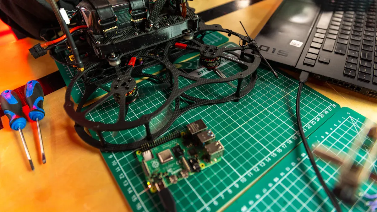
After drilling, components are put into the holes. Workers or machines do this job. Small parts are placed with tweezers or vacuum tools. Big jobs use AI plug-in machines and other equipment. It is important to put each part in the right way. Polarized components must face the correct direction. Leads need to go all the way in so the part sits flat. Sometimes, workers bend the leads or use tape to hold parts before soldering.
Good through hole technology means cleaning leads before putting them in. Heavy parts go near the center of the pcb to lower stress. Engineers make holes about 0.15mm bigger than the leads. These steps help stop problems and make pth assembly strong.
Soldering Methods
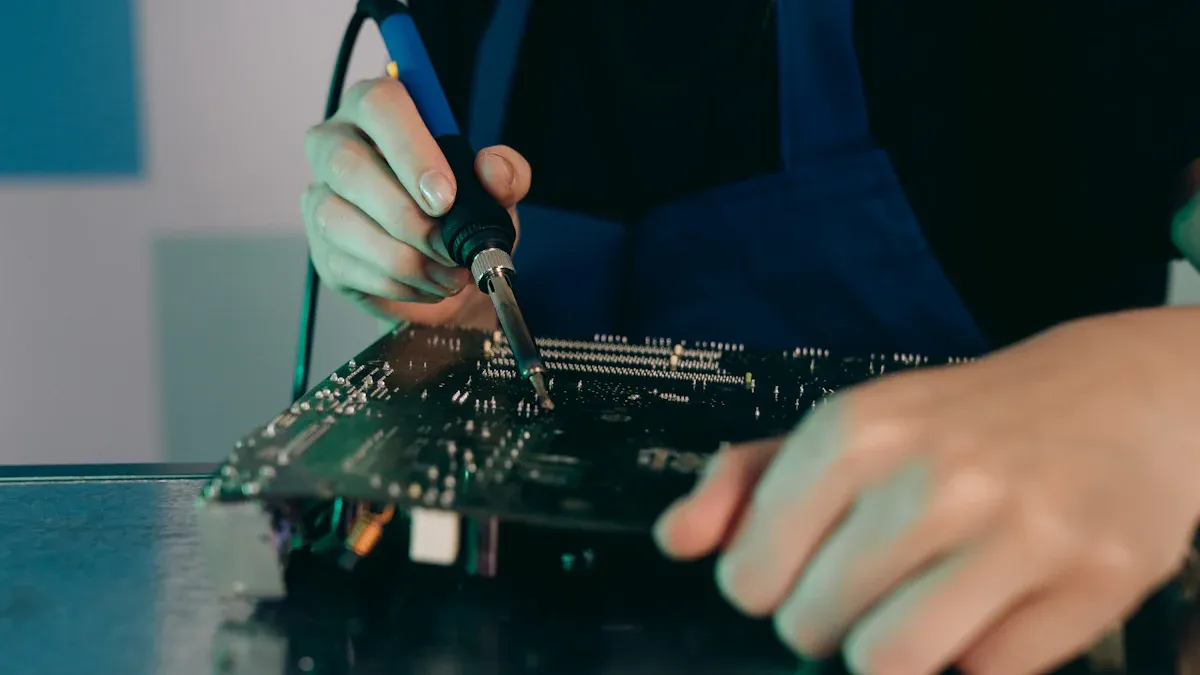
Soldering holds the leads to the pcb pads. Through-hole pcb assembly uses both hand and machine soldering. Hand soldering is used for small jobs or test boards. Workers heat the pad and lead at the same time. They put solder on the joint, not the iron tip. This makes a strong bond. Hand soldering needs skill and care.
Wave soldering is the main machine method in through hole technology. The pcb moves over a wave of hot solder after preheating and adding flux. This solders all the joints at once. Wave soldering is fast and gives steady results. It is best for making many boards. Selective soldering is used when both through-hole and surface-mount parts are on the board. It only solders the through-hole parts.
Aspect | Manual Soldering | Wave Soldering |
|---|---|---|
Reliability | Variable quality; operator skill dependent | Consistent, reliable joints; controlled process |
Throughput | Slower, labor-intensive | High efficiency; suitable for large-scale production |
Heat Control | Difficult to control temperature | Controlled preheating and soldering stages |
Quality Consistency | Inconsistent | Stable and repeatable |
Defect Rate | Higher | Lower; can approach zero-defect soldering |
Suitability | Small batches or rework | Large-scale production |
Wave soldering lowers defects and keeps boards clean. Some spots may need hand touch-ups if blocked by jigs. LTPCBA uses both ways to fit each pcb project. The company sets the conveyor angle, wave height, and temperature for full solder coverage.
Inspection and Quality Control
Checking and controlling quality is very important in through-hole pcb assembly. LTPCBA follows world rules like IPC-2221, IPC-7251, and IPC-A-610. These rules say how big holes and pads should be and what good solder joints look like. IPC-A-610 puts assemblies into three classes by how reliable they must be. Class 3 is the strictest and is used for things like planes, the army, and hospitals.
Description | Relevance to Through-Hole PCB Assembly | |
|---|---|---|
Class 1 | General electronics; lowest reliability | Basic soldering and placement standards |
Class 2 | Industrial electronics; moderate reliability | Moderate inspection rigor |
Class 3 | High-performance; highest reliability | Strict acceptance criteria |
Important checks include looking at solder joints, fillet shape, strength, and where parts are placed. Automated Optical Inspection uses cameras and software to find missing parts, wrong placement, and solder problems. X-ray inspection looks at hidden solder joints and inside the pcb. In-circuit testing checks if the board works and if parts are right. 3D AOI and laser tools give detailed views of solder joints.
Common problems in through hole technology are gaps in solder, solder balls, cold joints, solder bridges, and parts moving. AOI, X-ray, and flying probe tests help find these problems. LTPCBA uses top inspection tools and strict checks to make sure every pcb is good.
Note: LTPCBA always checks quality and follows world rules to make sure every through-hole pcb assembly is reliable.
Through Hole Technology Advantages and Applications
Advantages of Through Hole Assembly
Through hole technology gives designers strong and safe connections.
Through-hole pcb assembly makes strong joints because leads go through the board.
These joints help products last through shaking, bumps, and high heat.
Through hole assembly is easy to solder by hand, fix, or change.
This method is good for testing because engineers can swap parts fast.
Through-hole pcb assembly gives steady electrical links between layers, so it is used in military, planes, and factories.
Through hole technology helps products last in tough places.
Disadvantages and Limitations
Through-hole pcb assembly has some problems too.
Drilling holes in the board takes longer and costs more money.
Through hole assembly uses bigger parts, so fewer fit on the board.
Designers cannot put parts on both sides, so the board holds less.
Many holes make less space for wires and can make the board weaker.
Through hole technology is not good for tiny or high-speed designs.
Long leads can change signals because they add inductance and capacitance.
Limitation Aspect | Explanation |
|---|---|
Larger Component Size | Through-hole pcb assembly needs bigger holes and leads, using more pcb space. |
Longer leads in through hole assembly can cause signal problems at high frequencies. | |
Reduced Board Space Utilization | Drilled holes limit routing and component density. |
Labor-Intensive Assembly | Manual soldering and insertion slow down production. |
Typical Components and Use Cases
Through hole technology works best for big or heavy parts.
Transformers, semiconductors, and big capacitors use through-hole pcb assembly.
Switches, connectors, and battery holders need strong joints, so engineers pick through hole assembly.
Military, planes, and factory machines use through-hole pcb assembly for strength.
Medical tools, power supplies, and test gear also use through hole technology.
People making new things or testing ideas like through hole assembly for easy changes.
Reason for Preference in Through-Hole PCB Assembly | |
|---|---|
Military and Aerospace | Needs strong mechanical bonds and reliability under harsh conditions. |
Automotive Electronics | Must endure vibration and thermal cycling. |
Industrial Machinery | Handles high power and tough environments. |
Medical Devices | Requires accuracy and reliability. |
Power Supplies | Supports high voltage and current. |
Prototyping and R&D | Allows easy manual soldering and fast revisions. |
LTPCBA and Through-Hole PCB Assembly
LTPCBA is very good at through-hole pcb assembly because it uses new tools and checks quality.
The company follows ISO 9001, IPC-A-610, and UL rules for every board.
LTPCBA uses AOI, X-ray, and in-circuit tests to check soldering and assembly.
Customers get fast help, free checks, and quick answers to problems.
The team does everything from planning to shipping, making sure every board is good.
LTPCBA can make samples, small batches, and hard projects.
When you compare through hole assembly and surface mount technology, both are useful.
Through-hole pcb assembly is strong and easy to fix, so it is best for tough jobs and testing.
Surface mount technology fits more parts on the board, is faster, and costs less for big orders.
The good and bad sides of through-hole pcb assembly help engineers choose the best way for each board.
Many new boards use both ways to get the right mix of strength, size, and price.
Through hole technology uses drilled holes for component leads. This makes strong connections in pcb assembly.
The main steps are drilling, putting in parts, soldering, and checking.
Through-hole pcb assembly is very reliable and easy to fix. It also works well with high-power parts.
Many industries pick through hole assembly for important pcb jobs.
LTPCBA checks quality with new tools, strict rules, and expert help for every pcb project.
Advantages of Through-Hole PCB Assembly | Typical Applications |
|---|---|
Aerospace | |
Easy repair and replacement | Automotive |
Reliable in harsh environments | Industrial control |
FAQ
What is the main difference between through hole technology and surface mount assembly?
Through hole technology puts leads into drilled holes on the pcb. Surface mount assembly sticks parts right onto the board’s top. It does not use holes.
Why do engineers choose through-hole components for some pcb projects?
Engineers pick through-hole parts for strong bonds. Through hole pcb assembly is good for places with lots of shaking. It also makes fixing or swapping parts easy.
What are the pros and cons of through-hole pcb assembly?
Through-hole pcb assembly makes strong links and is easy to fix. But pth assembly uses more space and fits fewer parts on the pcb.
See Also
Complete Overview Of Through-Hole PCB Assembly Techniques
Choosing Between SMT And Through-Hole PCB Assembly Methods
Selecting The Best Through-Hole PCB Assembly For Industrial Use
Evaluating Reliability Of Through-Hole Versus SMT PCB Assembly
In-Depth Guide To DIP Cable And Through-Hole PCB Connections