How to Design Reliable Pads for Through-Hole Components

You can make strong through-hole component pads by following some steps. First, use IPC-2221 and IPC-2222 standards. These help you with pcb footprint, hole size, and pad math. Pick the right pad size for each through-hole part. Make sure the pad is strong and works well in the circuit. Good pads help stop problems when making the pcb. Look at the table below for common rules on through-hole parts and pad design.
Key Takeaways
Follow IPC standards like IPC-2221 and IPC-2222 to choose the right pad and hole sizes for each through-hole component. This ensures strong solder joints and reliable connections.
Make sure the annular ring around the hole is wide enough to prevent pad breakouts and weak joints. A strong ring and proper plating help your PCB last longer and handle stress.
Always check your design with your PCB maker to confirm drill sizes and clearances. This avoids mistakes, reduces costs, and guarantees your board is easy to build and repair.
Through-Hole Component Basics

Types of Through-Hole Components
There are many through-hole components in today’s pcb assemblies. Some examples are resistors, capacitors, inductors, connectors, diodes, LEDs, transformers, and power resistors. These parts are used when the pcb needs to be strong or handle lots of power. Through-hole components are good for tough places like cars, planes, and factories.
You can sort through-hole components by their lead style:
Axial leaded components have leads on both ends in a straight line. You see this in carbon resistors, electrolytic capacitors, and some LEDs.
Radial leaded components have both leads coming out from one side. Inductors and ceramic disk capacitors use this style a lot.
Role of Through-Hole Pads
Through-hole pads are important in pcb design. These pads hold the component leads in place. They make a strong bond so the part does not move. When you put a lead into a plated through-hole, it makes a tough connection. This connection can handle shaking and bumps. The pad has copper around the hole. This gives enough space for solder. It helps you make good solder joints. It also makes sure the layers in your pcb connect well.
The pad size and hole diameter should fit the lead. This helps you get the right amount of solder and a steady connection. Good soldering pads help with high power and make fixing things easier. You also lower the chance of problems and help your circuit last longer.
PTH Plating and Reliability
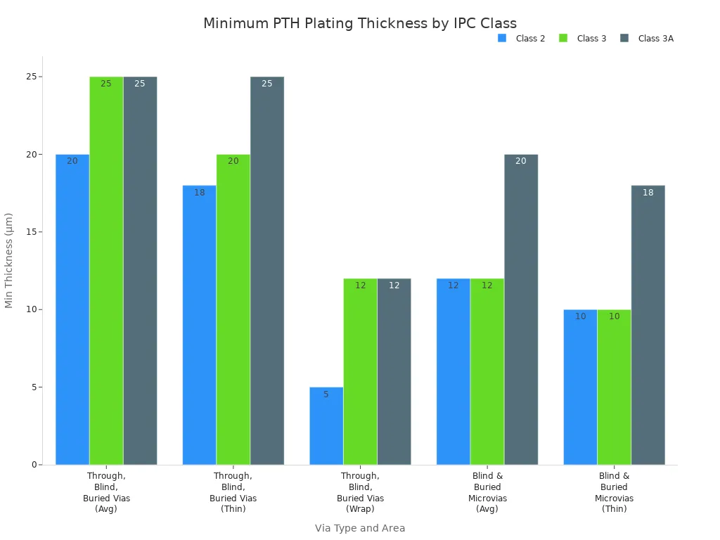
PTH stands for plated through-hole. This means there is copper inside the hole wall. The copper links the top pad to the bottom pad and any inside layers. You need to follow IPC rules for how thick the copper should be. For example, IPC 600J-Class 2 says you need at least 18 µm of copper. Many makers use 20 µm to be extra safe.
Good pth plating stops problems from heat, shaking, and water. You should not use npth for electrical connections. Good pad design, the right soldering pads, and strong plated through-holes help your pcb work better and last longer.
Through-Hole Pad and Hole Design

IPC Standards for Through-Hole Pads
When you make through-hole components, you need to use industry rules. These rules help your design work well and be easy to build. The IPC-2221 and IPC-2222 standards tell you how to pick pad size, hole size, and annular ring. IPC-2221 gives the main rules for all pcb types. IPC-2222 gives more details for hard or special boards. These rules help you stop problems like bad solder joints or pads coming off.
Aspect | IPC-2221 | IPC-6012E & Addendums | IPC-A-610 |
|---|---|---|---|
Lead-to-hole clearance | N/A | N/A | |
Annular ring size (Class 3) | N/A | Minimum 1 mil (inner layers), 2 mil (external layers) | N/A |
Plating thickness | N/A | N/A | |
Void allowance | N/A | No voids allowed in Class 3; Class 2 allows 1 void in 5% of holes | N/A |
Pad size calculation | N/A | Pad size = finished hole diameter + 2 × minimum annular ring + fabrication allowance | N/A |
Solder joint quality classification | N/A | N/A | Defines Class 1, 2, 3 solder joint quality levels with increasing reliability requirements |
You should always check which IPC class your pcb needs. Class 3 has the strictest rules and is used for things like planes and medical tools. Class 2 is used for most home and work electronics. IPC-A-610 helps you see if your solder joints are good for through-hole components.
Sizing PTH Holes and Pads
You need to pick the right hole and pad size for each part. First, measure the biggest lead on your part. IPC-2221 says you should have a 0.2 to 0.25 mm gap. This gap lets you put the lead in easily and helps solder flow. If the hole is too small, solder will not fill the space. If it is too big, the joint will be weak.
Source / Standard | Formula for Minimum Finished Hole Size (FHS) | Notes / Clearance Value |
|---|---|---|
FHS = Max Lead Diameter + 0.25 mm | Highest clearance level | |
IPC-2222 Level B | FHS = Max Lead Diameter + 0.20 mm | Medium clearance |
IPC-2222 Level C | FHS = Max Lead Diameter + 0.15 mm | Lowest clearance |
For example, if your lead is 0.8 mm, add 0.25 mm for the gap. The hole size is 1.05 mm. You round up to the next drill size, usually 1.1 mm. The pad should be big enough for a strong annular ring. IPC-2221 says the pad size is the hole size plus two times the smallest annular ring. Most of the time, you use a 2.1 mm pad for a 1.1 mm hole.
Lead Diameter (mm) | Hole Diameter (mm) | Pad Diameter (mm) |
|---|---|---|
0.8 | 1.1 | 2.1 |
You also need to think about the aspect ratio. This is how thick the pcb is compared to the hole size. Keep this number under 10:1 for good pth plating. If the hole is too deep for its width, the plating may not cover well. This can make weak spots.
Tip: Always ask your pcb maker what drill sizes and gaps they like. This helps you avoid mistakes and extra costs.
Annular Ring Requirements
The annular ring is the copper around the hole in the pad. This ring makes the pad strong and helps the part connect well. IPC-2221 and IPC-6012 say how wide the ring should be for each pcb class. For Class 2, the ring should be about 0.10 mm wide. For Class 3, it should be about 0.125 mm. You need a wide enough ring to stop pad breakouts and make strong solder joints.
IPC Class | Minimum Annular Ring Width | Notes |
|---|---|---|
Class 1 | ~0.05 mm (50 microns) | Least stringent, general electronic products |
Class 2 | ~0.10 mm (100 microns) | Dedicated service electronic products, higher reliability |
Class 3 | ~0.125 mm (125 microns) | High-performance electronic products, most stringent requirements |
If the ring is too thin, you can get bad solder joints, pads lifting, or open circuits. If the drill is off, the pad can break out, especially with a small ring. Always use enough copper around the hole to stop these problems.
Too little ring means less space for solder, which can cause bad joints and broken circuits.
Thin rings make the pcb weaker and can cause pads to break or crack.
You can also get higher resistance and signal problems.
Use teardrop pads to add more copper where the trace meets the pad. This makes the pad stronger and helps if the drill is not perfect.
Pad Shape and Connection to Planes
Most through-hole pads are round with a hole in the middle. This shape spreads copper evenly and gives good support. For plated through-hole pads, the copper inside the hole links the top and bottom layers, and sometimes the inside layers, too. This link is important for both power and strength.
Plated through-hole pads help solder flow from top to bottom, let you solder on both sides, and help move heat away.
Non-plated through-hole pads are only for holding parts and have extra space to stop shorts.
When you connect pads to inside planes, use thermal relief patterns. These patterns use thin lines to join the pad to the plane. Thermal relief helps control heat when you solder, so you get a good joint. Without thermal relief, the plane can take too much heat. This can make cold solder joints or make fixing the board hard.
Thermal relief makes building the board easier by stopping too much heat loss.
The number and size of the lines change how much power and heat can move.
Good thermal relief helps you solder well and fix things if needed.
You should know that through-hole pads and vias are not the same. Through-hole pads are for part leads and must be strong. Vias are smaller and just connect traces between layers. Vias do not need as much copper and are not made for lots of stress.
Note: Always check your pad design with pcb design software and use IPC-7351 for standard footprints. This helps you find mistakes before you build the board.
Step-by-Step Example: Calculating Pad and Hole Size
Let’s look at an example for through-hole parts:
Find the maximum lead diameter: Say your part has a 0.8 mm lead.
Add clearance: Use IPC-2221’s 0.25 mm. Hole size = 0.8 mm + 0.25 mm = 1.05 mm.
Select standard drill size: Round up to 1.1 mm.
Determine minimum annular ring: For Class 2, use 0.10 mm.
Calculate pad diameter: Pad diameter = 1.1 mm + (2 × 0.10 mm) = 1.3 mm. Many designers use 2.1 mm for extra safety.
Check aspect ratio: If your pcb is 1.6 mm thick, aspect ratio = 1.6 / 1.1 ≈ 1.45 (well below the 10:1 limit).
Verify with manufacturer: Make sure your drill and pad sizes match what your maker can do.
By following these steps, you make sure your through-hole pads meet IPC rules and give you strong soldering pads for all your through-hole parts.
You can make reliable through-hole pads by following IPC rules. Pick the right pad and hole size for your part. Check if your design can be made by your pcb maker. Always look at the pad plating, annular ring, and how strong the pad is. Use this checklist every time you design a pcb:
Checklist Item | Description |
|---|---|
Footprint alignment | Make sure the pad fits the part datasheet |
Annular ring width | Keep the ring wide enough for a strong pad |
Hole plating | Make sure the pad is plated for good soldering |
Solder mask clearance | Stop pads from touching each other |
Assembly clearance | Give space for tools to reach the pad |
Silkscreen legibility | Do not let the silkscreen cover the pad |
Test probe placement | Put test points close to the pad for checking |
If you balance pad strength, good connections, and easy building, your pcb will last a long time.
FAQ
What is the main reason for pad failures in through-hole designs?
Poor annular ring width or weak plating often causes pad failures. You should always check your pad size and plating thickness before sending your design for manufacturing.
How do you choose the right pad shape for a through-hole component?
You select the pad shape based on the component lead type.
Round pads fit most leads.
Teardrop pads add strength at trace connections.
Can you use the same pad size for all through-hole parts?
Component Type | Pad Size Needed? |
|---|---|
Resistor | No |
Connector | No |
Capacitor | No |
You must match each pad size to the specific lead diameter for best results.
See Also
Complete Handbook For Assembling Through Hole PCBs
Seven Essential Quality Checks For Expert Through Hole PCB Assembly
Evaluating Reliability Between Through Hole And SMT PCB Assembly