Stacked Microvias vs Staggered Microvias in PCB Design Explained
PCB microvias improve PCB designs by making layouts smaller and connections stronger. Stacked microvias are placed right on top of each other, while staggered microvias are positioned in different spots across layers. Understanding these differences enhances circuit density and signal quality. This knowledge leads to better designs for devices like phones and smartwatches.
Key Takeaways
Stacked microvias use less space by sitting one above another. They work well in small gadgets like phones and smartwatches.
Staggered microvias handle stress better and last longer. They are great for strong devices like medical tools and factory equipment.
Pick stacked microvias for saving space and clear signals. Choose staggered microvias for durability and lower costs.
Understanding PCB Microvias
What Are PCB Microvias?
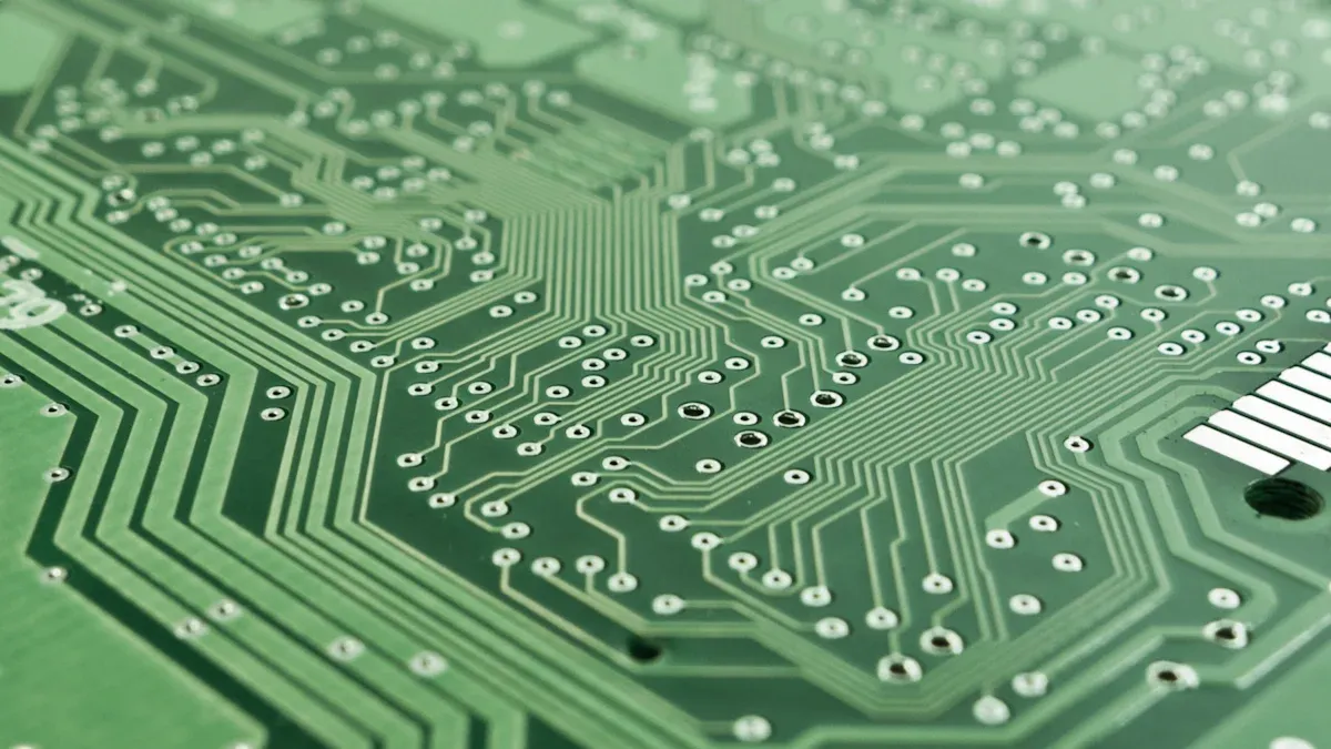
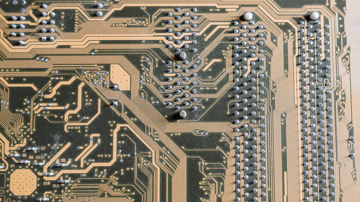
PCB microvias are tiny holes in circuit boards. They connect different layers, letting signals move between them. This helps create smaller and more complex designs. Microvias are very small, usually less than 150 µm wide. High-power lasers drill these tiny holes with great accuracy. Some microvias are stacked to link layers directly. Others are staggered to make them stronger.
Microvias are important in high-density interconnection (HDI) PCBs. These boards are used in small devices like phones and smartwatches. Microvias make connections smaller, saving space without losing performance. They also improve signal quality and reduce interference.
A webinar by EIPC stressed cleaning microvia pads during production. Clean pads stick better and work reliably, even as pad sizes shrink.
Why Are Microvias Important in PCB Design?
Microvias are key for modern PCB designs. They help fit more parts into smaller spaces. Microvias carry signals between layers, reducing interference and boosting performance. In HDI PCBs, they allow compact designs with advanced features.
Drilling and filling microvias carefully makes products last longer. Lasers drill precise holes, and proper filling makes them durable. This is why microvias are vital for reliable devices like medical tools and car electronics.
Microvias help PCBs by making them smaller, improving signals, and lasting longer. As technology grows, microvias become even more important.
Stacked Microvias: Features and Benefits
What Are Stacked Microvias?
Stacked microvias are tiny holes in a PCB. They are placed directly on top of each other across layers. These holes connect layers vertically, helping with compact designs. Engineers use lasers to drill them with great precision. Stacked microvias save space by using the same spot on each layer.
Studies show stacked microvias work well in simpler designs. For boards with many layers, mixing stacked and staggered microvias helps. This method makes connections stronger and reduces failure risks.
Key Characteristics of Stacked Vias
Stacked vias have special traits that make them different. These include:
Alignment: Microvias are stacked straight up, forming a vertical link.
Space Efficiency: They use less space, perfect for dense layouts.
Copper Filling: Copper is added to improve strength and conductivity.
The table below shows stacked vs staggered setups:
Configuration | Description | Benefits |
|---|---|---|
Stacked | Microvias align vertically, sharing the same x-y spot. | Easier vertical connections. |
Staggered | Microvias are offset, connecting layers in patterns. | Handles stress better and suits complex designs. |
Advantages of Stacked Microvias in High-Density Designs
Stacked microvias have many benefits for tight PCB layouts. They make vertical connections simple, saving space for more parts. This is great for small devices like phones and wearables. Their straight alignment keeps signals clear, which is key for fast systems.
Stacked vias also speed up production. Their simple design makes layouts easier to create. Adding copper boosts their strength and performance. These features make stacked microvias a top choice for modern PCBs.
Staggered Microvias: Features and Benefits
What Are Staggered Microvias?
Staggered microvias are tiny holes in a PCB. They connect layers in a spread-out pattern. Unlike stacked microvias, staggered vias are placed in different spots. This design lowers stress and makes them more reliable. Engineers use lasers to drill these holes carefully for accurate connections.
Staggered microvias work well in tough systems like medical devices. Their spread-out design handles stress better, avoiding damage. This makes them a good choice for boards with many layers in strong systems.
Key Characteristics of Staggered Vias
Staggered vias have special features that improve PCB designs:
Space Efficiency: Their spread-out design saves space on PCB layers.
Simplified Manufacturing: They are easier and cheaper to make than stacked vias.
Signal Integrity: Shorter paths keep signals clear and reduce distortion.
Stress Resistance: Spread-out stress lowers the chance of breaking or failing.
These features make staggered vias great for small devices like tablets and smartwatches.
Advantages of Staggered Microvias in Stress-Resistant Applications
Staggered microvias are best for systems needing strong and clear signals. Their spread-out design stops signals from mixing or interfering. This is important for tools like medical devices and factory machines.
The staggered layout also makes them tougher. It spreads stress across the board, handling heat and pressure better than stacked vias. This makes them perfect for boards used in hard conditions. If you need strong and reliable designs, staggered microvias are a smart choice.
Stacked Microvias vs Staggered Microvias: A Simple Comparison
Saving Space and Better Layouts
High-density PCBs need smart use of space. Stacked vias are great for saving space. They stack microvias straight up, using less room. This lets more parts fit in small devices like phones and watches.
Staggered vias spread out across layers, needing more space. This design handles stress better but limits tight layouts. The table below shows how stacked and staggered vias differ:
Feature | Stacked Vias | Staggered Vias |
|---|---|---|
Space Saving | Uses less space with vertical stacking. | Needs more room due to spread-out design. |
Making Process | Harder to make; needs careful alignment. | Easier to make; often skips copper filling. |
Cost | Costs more due to tricky production steps. | Cheaper with simpler manufacturing. |
Signal Quality | Great for clear signals in fast circuits. | Lowers signal mixing but may change impedance. |
Stress Handling | Can break under heavy stress. | Handles heat and pressure better. |
Signal Quality in Fast Designs
Good signals are key for fast PCBs. Stacked vias keep signals clear by controlling impedance. Their straight design stops unwanted effects, keeping signals clean. This makes them perfect for fast systems like phones and computers.
Staggered vias stop signals from mixing by spreading connections apart. But their design can slightly change impedance, affecting signal quality. HDI PCBs use microvias to match trace impedance, improving signal flow and reducing problems.
Strength and Long-Lasting Design
Strength matters when picking between stacked and staggered vias. Staggered vias are stronger because they spread out stress. This makes them good for tough devices like car tools and factory machines.
Stacked vias save space but can break under stress. They need more lamination cycles, which may lower durability. The table below compares their strength and making process:
Feature | Staggered Vias | Stacked Vias |
|---|---|---|
Strength | Stronger with fewer lamination cycles. | Weaker with more lamination cycles. |
Making Process | Easier and cheaper to make. | Harder and costs more to produce. |
Design Choices | Allows bigger holes and pads. | Limits design options. |
Making and Cost Differences
Stacked vias are harder to make because they need careful alignment and copper filling. This makes them cost more, but their space-saving design is worth it for tight layouts.
Staggered vias are easier to make and often skip copper filling. This lowers costs and improves production speed. If saving money is important, staggered vias are a better choice.
Picking the Right Vias
Choosing between stacked and staggered vias depends on your PCB needs. Stacked vias are best for saving space and keeping signals clear. They work well in small, fast designs.
Staggered vias are better for strong and affordable designs. They handle stress well and cost less to make. Knowing the pros and cons of each type helps you pick the right one for your project.
Design and Manufacturing Considerations with LTPCBA
Aspect Ratio and Layer Count
When making PCBs, think about the microvia aspect ratio. This compares how deep the via is to its width. If the ratio is too high, it can cause problems like bad plating. To avoid this, keep the ratio at 10:1 or lower. This helps make the PCB work better, especially in fast designs.
Using microvias or buried vias can control high aspect ratios. Follow rules for via size and spacing to avoid issues. For example:
Keep the aspect ratio at 1:1 or less for good plating.
Make sure via sizes and spacing meet the smallest allowed limits.
By following these tips, you can reduce unwanted effects and improve signals in your PCB.
Sequential Lamination and Copper Filling
Sequential lamination is important for making multi-layer PCBs. It joins layers together into one strong board. Aligning layers correctly during lamination keeps signals clear and vias connected. Using the right pressure stops gaps and ensures strong bonding.
Prepreg materials are key in this process. They stick layers together, insulate them, and control thickness. Good prepreg quality affects how well the PCB works. Adding copper to microvias makes them stronger and better at carrying signals. These steps help your PCB work well even in tough conditions.
How LTPCBA Ensures Quality in Microvia Manufacturing
At LTPCBA, we focus on making high-quality microvias. Our advanced tools drill precisely and keep aspect ratios correct. We follow global standards to make reliable PCBs. Our skill in lamination and copper filling makes designs stronger and better. With LTPCBA, your PCBs will meet top industry standards.
Electrical Performance of Stacked and Staggered Microvias
Signal Integrity in High-Speed PCB Designs
Keeping signals clear is very important in fast circuits. Bad signals can cause errors and make the PCB fail. Stacked microvias are lined up straight, which keeps signals steady. This makes them great for fast circuits needing clear signals.
To make circuits work well, control impedance and pick good materials. Using the right materials stops signal mixing and power changes. Also, plan trace lengths and via spots carefully to avoid signal problems. These steps help create strong designs for today’s fast circuits.
Managing Thermal and Mechanical Stress
Heat and stress can harm your PCB and make it fail. Staggered microvias are better at handling stress because they spread it out. This lowers the chance of cracks or damage in tough conditions.
Good heat control uses thicker copper, thermal vias, and heat sinks. These tools help remove heat and keep the PCB cool. Rules like IPC-2152 guide how to handle heat based on copper and current. Testing parts in real conditions also avoids too much stress. These steps make your PCB stronger and last longer.
Applications of Stacked and Staggered Microvias
Use Cases for Stacked Microvias
Stacked microvias are great for saving space in small designs. They are used in HDI PCBs for compact devices like phones and tablets. These microvias let engineers stack layers, adding features without taking up space.
In telecom, stacked microvias keep signals clear for fast data transfer. They work well in 5G networks and high-speed systems. Their precise alignment reduces signal problems, making them ideal for these uses. They are also perfect for multilayer PCBs with 10+ layers, where space is tight.
In cars, stacked microvias are key for electronics like ADAS and EVs. These systems need small, powerful PCBs to work safely and quickly. Stacked microvias help process data reliably in these advanced systems.
Use Cases for Staggered Microvias
Staggered microvias are best for tough and cost-friendly designs. Their spread-out layout handles stress, making them reliable in harsh conditions. Medical devices like monitors and diagnostic tools use staggered microvias. These devices need to work well under heat and pressure, which staggered vias can handle.
In factories, staggered microvias are used in machines and automation systems. They resist heat and stress, lasting longer in hard environments. They are also cheaper to make, needing less plating and simpler processes. This makes them a good choice for large-scale production.
Here are some benefits of staggered microvias:
Cost Efficiency: Less plating time means lower costs.
Reliability: Better performance data than stacked microvias.
Collaboration: Working with fabricators improves designs and saves money.
Industry Trends and Examples with LTPCBA
Microvias are in high demand as industries need smaller, faster PCBs. At LTPCBA, we use advanced tools and strict quality checks to meet these needs. Our microvia solutions ensure top performance and reliability.
Aspect | Details |
|---|---|
Projected Advancements | New laser tools make smaller microvias with better ratios. |
Contribution to Miniaturization | Microvias connect dense circuits, saving space while keeping features. |
Role in HDI & Multilayer PCBs | Reliable microvias support PCBs with 6-12+ layers. |
Manufacturing Experience | LTPCBA makes thousands of microvia boards every year. |
Quality Control | Full inspections ensure high standards for all applications. |
Fast Prototypes | LTPCBA delivers quick prototypes and handles big orders too. |
Microvias are vital in industries like telecom, electronics, cars, and healthcare. For example:
Industry | Applications |
|---|---|
Fast networks and small designs. | |
Consumer Electronics | Advanced phones and wearables with complex circuits. |
Systems like ADAS and EVs needing compact PCBs. | |
Medical Devices | Tools like monitors and diagnostic machines. |
By working with LTPCBA, you get advanced microvia solutions for your needs. Whether for quick prototypes or large orders, we ensure your PCBs meet today’s tech demands.
Stacked microvias use less space and keep signals clear. Staggered microvias are stronger under stress and cost less to make. Think about space, strength, and cost when picking the best type.
LTPCBA uses advanced tools and strict rules to make great microvias. Their solutions help create strong and efficient PCB designs.
FAQ
What makes stacked and staggered microvias different?
Stacked microvias go straight up, while staggered microvias spread out. This changes how much space they use, how strong they are, and how hard they are to make.
Which microvia type is best for fast circuits?
Stacked microvias are better for fast circuits. Their straight design keeps signals clear and avoids mixing, making them great for quick data transfer.
How does LTPCBA make sure microvias are high quality?
LTPCBA uses special tools, careful drilling, and strict checks. These steps make sure microvias are strong and meet top global standards.
See Also
Key Technical Challenges for PCB Boards in SMT Assembly
Effective Strategies for Optimizing SMT Lines in PCBA
Evaluating Advantages and Disadvantages of SMD vs. Through-Hole
Clarifying SMT and DIP Assembly Techniques for PCBA
Designing PCB Boards for Enhanced SMT Manufacturing Efficiency