The role of SPI visual inspection after SMT solder paste screen printing in the production of PCBA products
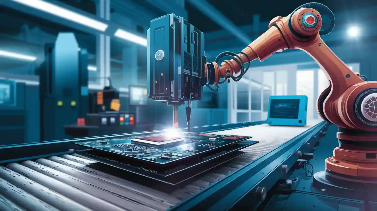
SPI visual inspection is very important in making PCBAs. It checks if solder paste deposits are of good quality. Finding problems early helps lower mistakes and keeps quality high. This also saves time by reducing fixes, helping you get good results every time.
Key Takeaways
SPI checks make sure solder paste is applied correctly, avoiding mistakes and making products more reliable.
Finding solder paste problems early saves time and money by cutting down on fixes and speeding up production.
Using advanced SPI tools in factories makes work smoother, reduces errors, and helps make products faster.
Understanding SPI Visual Inspection in PCBA Production
What is SPI visual inspection and why is it essential?
SPI visual inspection checks the quality of solder paste on PCBs. It ensures the paste applied during printing meets exact standards. This is important because solder paste helps place and connect components. If the paste is uneven, it can cause bad connections or short circuits.
Why is this process so important? It finds problems early. For example, a German company had high costs due to manual checks. After using an automated SPI system, they cut flaw detection time by 70%. This improved product quality and made customers happier. SPI inspection not only improves quality but also saves time and money.
As PCBs become more complex, SPI inspection is even more needed. It ensures solder paste is applied correctly, which is key for modern electronics to work well.
The role of SPI in ensuring solder paste quality
SPI systems help keep solder paste quality high. They measure things like height, area, and volume of the paste. These checks make sure the paste is spread evenly on PCB pads. For example, measuring height avoids too little solder, and volume checks ensure even joints.
Here’s how SPI systems help with quality:
Function | Description |
|---|---|
Solder paste height measurement | Measures solder paste height on PCB pads with great accuracy. |
Solder paste area measurement | Checks the paste coverage area to avoid it being too small or big. |
Volume measurement | Calculates paste volume to ensure every joint is consistent. |
Defect detection | Spots misprints, offsets, or shape issues that could cause problems. |
By focusing on these areas, SPI inspection reduces defects and ensures solder paste meets standards. This is crucial in industries where even small mistakes can cause big problems.
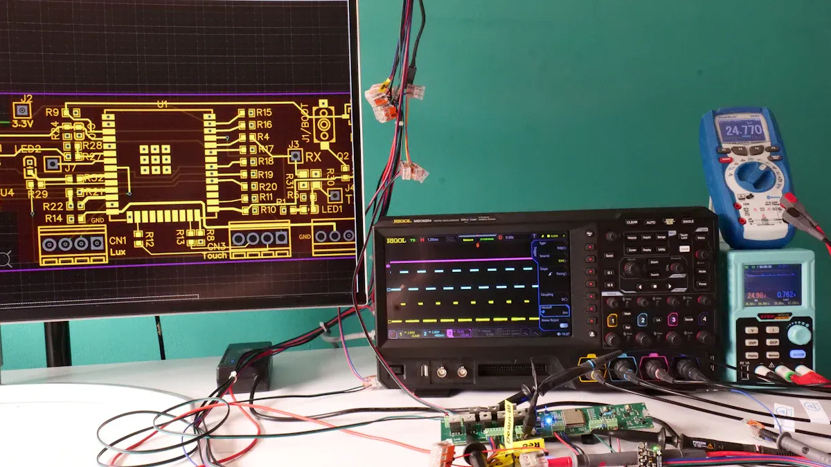
Advanced technologies used in SPI systems
Modern SPI systems use advanced tools for better results. These include 3D imaging, laser scanning, and machine learning. For instance, 3D imaging creates detailed models of solder paste to measure height, area, and volume. Laser scanning makes inspections faster and more accurate. Machine learning finds flaws by studying patterns and differences.
Automation in electronics has made SPI systems even better. Automated systems reduce human mistakes and speed up inspections. This is important to meet the demand for high-quality electronics.
The Process of SPI After SMT Solder Paste Screen Printing
Key steps in SPI visual inspection
SPI visual inspection follows clear steps to check solder paste. Each step helps find and fix problems early. Here’s a simple breakdown:
Step | Description |
|---|---|
Image capture | A camera takes clear pictures of the solder paste on the PCB. |
Image analysis | The system studies these pictures to check the paste’s shape and size. |
Problem detection | It spots issues like uneven paste or misalignment by comparing to standards. |
These steps make sure the solder paste is applied correctly. Catching problems early keeps production smooth and quality high.
How SPI evaluates solder paste deposits
SPI systems use smart tools to check solder paste. They measure important things like volume, height, area, and position. Each check shows how well the paste is applied.
Measurement Tool | Description |
|---|---|
3D Measurement Tools | Measures the height and volume of solder paste for detailed checks. |
Automated Software | Quickly finds mistakes in paste application using captured images. |
When checking solder paste, the system looks at:
Volume: Makes sure there’s enough paste for a strong bond.
Height: Checks that the paste isn’t too thin or thick.
Area: Ensures the paste covers the pad properly.
Position: Confirms the paste is placed in the right spot.
By focusing on these, SPI ensures the solder paste is always reliable and consistent.
Integration of SPI systems into the SMT production line at LTPCBA
At LTPCBA, SPI systems are part of the SMT production process. They check solder paste right after it’s printed. This helps catch problems before moving to the next step.
The automated SPI systems need little human help, lowering mistakes. Tools like 3D imaging and machine learning make inspections more accurate. By using these systems, LTPCBA ensures top-quality PCB assembly.
Tip: Adding SPI systems to your production line can cut down defects and boost efficiency.
Benefits of SPI Visual Inspection for PCBA Manufacturing
Improving solder paste quality and reliability
SPI visual inspection helps make solder paste more reliable. It checks important things like height, volume, and area. This ensures the paste is applied evenly every time. Good solder paste application prevents problems like weak joints or short circuits. These issues can harm how your PCBA products work.
A comparison shows how better solder paste improves results. A thinner foil thickness (4 mil) in experimental paste had a smaller CV range. It also printed better than the control paste. This led to fewer defects overall.
Solder Paste Type | Foil Thickness | CV Range (%) | Print Capability | Defect Rate |
|---|---|---|---|---|
Control | 5 mil | 25 - 45 | Poor | High |
Experimental | 4 mil | 5.8 - 7.0 | Good | Low |
Using SPI systems can give you similar results. They help improve solder paste reliability and ensure high-quality PCB assemblies.
Cutting defects and lowering rework costs
Finding problems early saves both time and money. SPI systems catch issues like misalignment or not enough solder paste before parts are added. This reduces expensive fixes later in production.
Data shows fixing defects later costs much more. Finding a problem during SPI costs $0.40. But finding it during AOI or FA can cost 11,000% or 3,000% more.
Stage of Detection | Cost of Defect | Increase in Cost |
|---|---|---|
SPI | $0.40 | - |
AOI | $45 | 11250% |
FA | - | 3000% |
Adding SPI systems helps catch problems early. This lowers rework costs and boosts profits.
Boosting production speed and saving money
SPI visual inspection makes production faster by automating checks. Machines quickly review solder paste, cutting inspection time. This also removes human mistakes, keeping results consistent.
Catching problems early also saves money. Fixing issues later can cause delays and extra costs. SPI systems streamline production, making high-quality PCBAs at lower costs.
At LTPCBA, SPI systems are part of the SMT production line. They ensure solder paste quality while keeping production fast. Using similar systems can help you save time and money in your manufacturing process.
Addressing Challenges in SPI Visual Inspection
Common challenges in implementing SPI systems
Using SPI systems can be tricky at times. For example, a smart watch company spent $200,000 yearly fixing mistakes. They only used AOI for checks and skipped SPI. This caused solder paste problems that led to defects later.
Here are some common SPI system challenges:
Challenge Type | Description |
|---|---|
Fast signals can get mixed up, causing errors in data. | |
Timing Mismatches | Wrong clock settings can mess up SPI communication. |
Hardware Compatibility | Devices with different needs make it hard to connect properly. |
Processing Overhead | Poor management can slow down SPI communication, hurting performance. |
These issues show why setting up and maintaining SPI systems is so important.
Strategies to optimize SPI performance
You can make SPI work better by adjusting key settings. Fixing these settings makes the process more reliable and cost-effective. Operators can also use data and experience to improve results. For example:
Matching team goals with management using clear performance indicators.
Using advanced tools to lower mistakes and work faster.
These steps help improve production and make everything run smoothly.
How LTPCBA ensures effective SPI integration
At LTPCBA, SPI systems are part of the SMT production process. Tools like 3D imaging and machine learning check solder paste carefully. Automated systems reduce mistakes and make inspections more accurate. By solving problems early, LTPCBA keeps quality high and products reliable.
Note: Adding SPI systems can lower defects and speed up production, saving both time and money.
SPI visual inspection is key to making good PCBAs. It finds problems early, improves solder joints, and lowers mistakes. Here’s how it helps production:
Early problem detection stops bigger issues later.
Proper solder paste use makes strong connections.
Fewer mistakes mean less fixing costs.
Better processes make production faster.
Higher first-pass success improves efficiency.
Catching issues early saves money and resources.
At LTPCBA, advanced SPI tools keep quality steady. They help meet industry rules and customer needs.
FAQ
What does SPI visual inspection do?
SPI checks solder paste quality by measuring height, volume, and position. It finds problems early, helping make reliable PCBs.
How does SPI make production faster?
SPI systems check solder paste automatically, saving time and avoiding mistakes. Catching problems early means less fixing and lower costs.
Why add SPI to your production line?
Adding SPI ensures solder paste is applied evenly and correctly. It reduces errors, improves quality, and meets industry standards easily.
See Also
Essential Factors For Effective Solder Paste Screen Printing In SMT
The Impact Of Solder Paste Quality On PCB SMT Soldering
Understanding SMT And DIP Assembly In PCBA Processes
Exploring Industrial Serial Screen PCBA Applications Today
The Influence Of Reflow Soldering Temperature On PCB Quality