How does SMT assembly achieve double-sided mounting
Surface mount technology has revolutionized electronics by enabling double-sided mounting. This process allows components to be placed and soldered on both sides of a double-sided PCB. It requires precision, specialized tools, and strict quality control. LTPCBA excels in double-sided SMT assembly, offering advanced solutions to meet your assembly needs with reliability and expertise.
Key Takeaways
Double-sided SMT assembly places components on both sides of a PCB using precise steps like solder paste application, component placement, reflow soldering, and careful board flipping to protect parts.
Strong process control and advanced inspection methods help prevent defects and ensure high-quality results in double-sided SMT assembly.
Using double-sided PCBs allows for smaller, more complex electronic designs with higher circuit density, making devices more compact and reliable.
Double-Sided SMT Process
Double-sided SMT assembly lets you place electronic components on both sides of a double-sided PCB. This process uses a series of precise steps to make sure every component is secure and every connection is strong. LTPCBA uses advanced techniques in double-sided smt assembly to deliver reliable results for your projects.
Solder Paste Application
You start the process by applying solder paste to the pads on the first side of the PCB. This step uses a stencil that matches the pad layout. The stencil ensures the right amount of solder paste goes onto each pad. The thickness and shape of the stencil control how much paste is deposited. If you use too little or too much, you risk defects like tombstoning or poor solder joints.
Metric | Definition | Importance |
|---|---|---|
Ratio of stencil opening to side wall area | AR > 0.66 is needed for good printing | |
Transfer Efficiency | Volume of paste deposited vs. stencil volume | Ideal is 100% for consistent solder joints |
Consistency (Std Dev) | Variation in transfer efficiency across pads | ≤ 10% ensures uniform solder paste application |
Solder Paste Inspection | Machines measure paste height, width, and volume | Detects missing paste or bridges before defects |
Solder Paste Inspection (SPI) checks the paste after application. SPI machines use 2D or 3D imaging to measure the paste’s height, width, and volume. This step helps you catch problems early, reducing the risk of defects later in the smt assembly process.
Component Placement
After you apply the solder paste, pick-and-place machines position the components onto the pasted pads. These machines use vision systems to make sure each part is placed accurately. High-speed pick-and-place systems can handle thousands of components per hour. Precise placement is important because it reduces defects and improves the yield of your smt assembly.
Tip: Grouping similar components and minimizing machine head travel can speed up the process and improve accuracy.
Sometimes, you may need to place large or special components by hand. After placement, a quick visual inspection helps you spot any missing or misaligned parts before moving to the next step.
Reflow Soldering
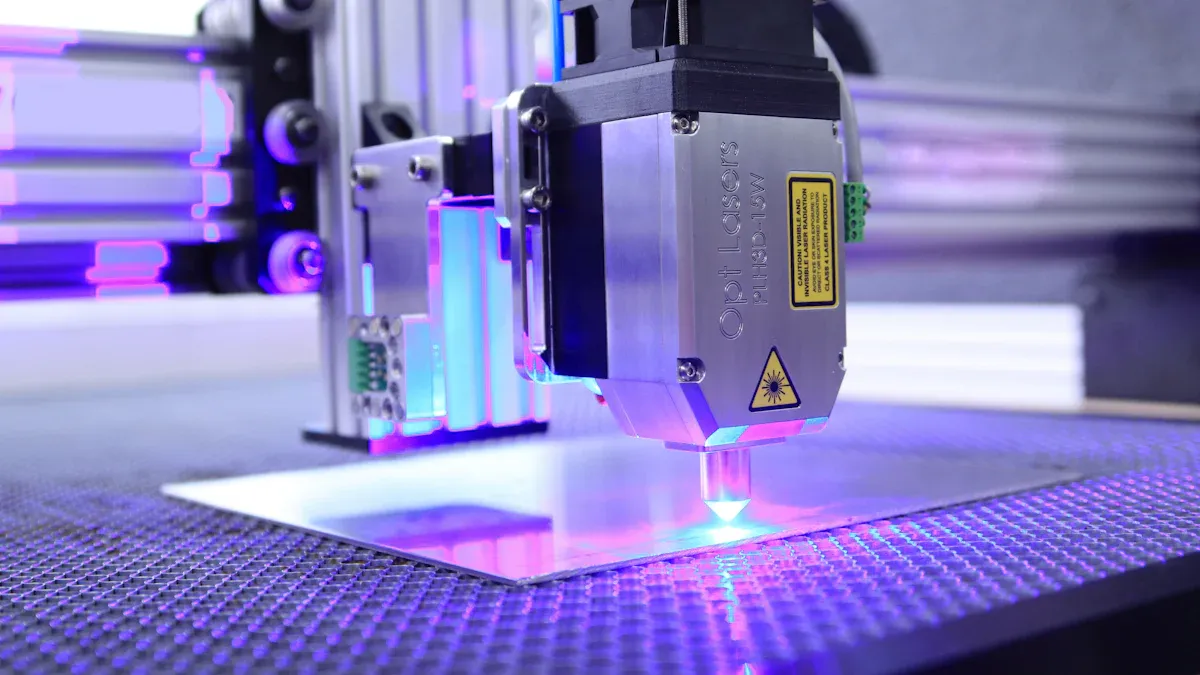
Now, you move the board into a reflow oven. The oven heats the board in several stages: preheating, soaking, reflow (where the solder melts), and cooling. The solder paste melts and forms strong connections between the component leads and the PCB pads. For lead-free solder, the temperature usually reaches about 217°C, but it should not go above 250°C to avoid damaging sensitive parts.
A well-controlled temperature profile is key. If you heat the board too quickly or too slowly, you risk poor solder joints or damaged components. LTPCBA uses advanced ovens and precise temperature control to ensure high-quality results in double-sided smt assembly.
Board Flipping
Once the first side is complete, you need to flip the board to work on the second side. This step requires care. You must protect the components already soldered on the first side. Special fixtures or carriers elevate the PCB, so the first-side components do not touch the work surface. This method keeps the first side safe from damage during the second side process.
Technical studies show that proper board flipping and support help preserve the integrity of solder joints and micro-vias. This approach simulates real-world stresses and ensures your double-sided PCB remains reliable.
Second Side Assembly
You repeat the process for the second side. First, you apply solder paste using a stencil. SPI checks the paste for accuracy. Then, pick-and-place machines add the second side components. Sometimes, you use adhesives to hold small or lightweight parts in place. This step is important because the second side will face downward during the second side reflow soldering process.
Note: Using adhesives and careful process control helps prevent components from falling off or shifting during reflow.
LTPCBA’s expertise in second side component placement and process control ensures that both sides of your double-sided PCB meet strict quality standards.
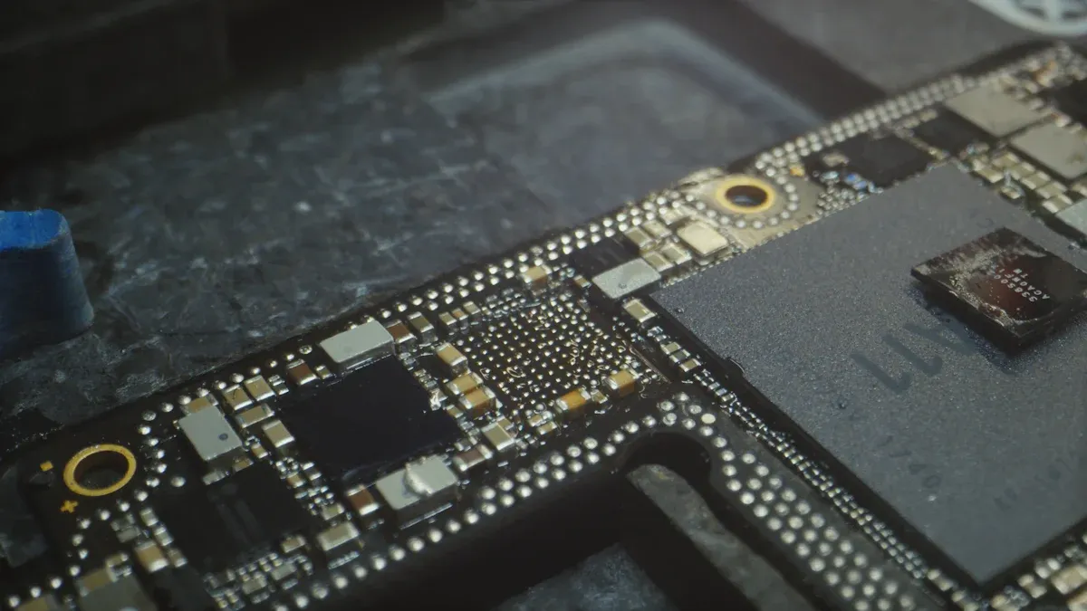
Inspection and Testing
After both sides are assembled and soldered, you inspect the board for defects. Automated Optical Inspection (AOI) systems use high-resolution cameras to check for missing parts, misalignment, solder bridges, and other issues. For complex boards, X-ray inspection can reveal hidden defects inside solder joints, especially under BGAs or fine-pitch components.
You also perform in-circuit tests (ICT) to check for electrical shorts or opens. Functional tests verify that the assembled PCB works as intended. These steps are critical in double-sided smt assembly to guarantee reliability and performance.
LTPCBA uses a combination of SPI, AOI, and functional testing to deliver high-quality smt assembly. Their commitment to quality assurance and advanced techniques in double-sided smt assembly ensures your products meet the highest standards.
SMT Assembly Challenges & Solutions
Alignment & Placement
You may face alignment and placement issues during double-sided SMT assembly. These problems can cause defects like tombstoning or solder bridging. Advanced SMT machines use vision systems to align the PCB and stencil. These systems find fiducial marks and make micro-adjustments, so components land in the right spot. Pick-and-place machines also check each part’s orientation and position. Keeping these machines calibrated helps you avoid many placement errors. Most defects in SMT assembly come from poor solder paste printing, so using the right stencil and alignment tools is key.
Common challenges of double-sided smt assembly include:
Component warpage from thermal stress
Tombstoning due to uneven heating
Solder bridging from misalignment
Voids in solder joints from contamination
Thermal Management
Double-sided SMT assembly creates extra heat challenges. When you reflow the second side, the first side’s components can get too hot. Studies show that using heat shields during rework protects sensitive parts. Placing a square-shaped heat shield at the heat source lowers peak temperatures by over 8%. This step reduces solder joint cracks by more than half. You can use thermal cameras and sensors to check heat spread and keep all components safe.
Process Control
You need strong process control to keep double-sided SMT assembly reliable. Most solder defects start with stencil printing. You should track these process metrics:
Metric / Parameter | Description / Role |
|---|---|
Defect Rate from Stencil Printing | |
Area Ratio (AR) | Ensures enough solder paste for strong joints on both sides. |
Transfer Efficiency | Measures how much solder paste transfers through the stencil. |
Solder Paste Inspection (SPI) | Finds missing or extra solder paste early in the process. |
Standard Deviation of Paste Volume | Shows if your printing process is stable and controlled. |
Using these metrics, you can spot problems early and fix them before they affect your SMT assembly.
LTPCBA Quality Assurance
LTPCBA stands out in SMT assembly by following strict quality standards. The company holds certifications like ISO, IATF, UL, and IPC-A-610. You benefit from advanced inspection methods, including AOI, X-ray, and electrical testing. LTPCBA also uses burn-in and thermal shock tests to check long-term reliability. These steps ensure your double-sided assemblies meet the highest standards for safety and performance.
Benefits & Applications
Higher Density
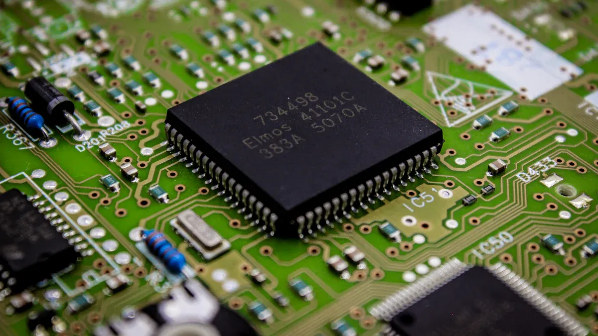
You can fit more components on a double-sided PCB than on a single-sided board. Double-sided smt assembly lets you use both sides of the board, which increases circuit density. This means you can design smaller products without losing performance. Many engineers use double-sided boards to save space and reduce the size of electronic devices. You get more functions in a compact design, which is important for modern electronics.
Complex Designs
Double-sided smt assembly supports advanced and complex circuits. You can place components on both sides, which helps you manage heat and avoid interference. Technical documents like stencil aperture files, design rule check reports, and netlist files help you plan and check your design. You also use fabrication notes and layer stack-up information to make sure your board meets all requirements. The process includes careful placement, controlled soldering, and thorough inspection. This approach lets you build reliable and high-performance products.
Tip: Double-sided smt assembly is ideal for circuits that need high reliability, thermal management, and signal integrity.
LTPCBA Service Advantages
You benefit from LTPCBA’s expertise in double-sided smt assembly. The company offers quick response times and a high pass rate. You get support from a team that uses advanced inspection tools and follows strict quality standards. LTPCBA serves many industries, such as automotive, telecommunications, and consumer electronics. You can trust LTPCBA to deliver reliable smt assembly for both simple and complex projects.
Typical Application | Benefit of Double-Sided SMT | |
|---|---|---|
Automotive | Sensor modules | High reliability, compact design |
Consumer Electronics | Smart devices, wearables | Miniaturization, more features |
Telecommunications | Network equipment | High-frequency, dense circuits |
You achieve double-sided mounting through a careful process:
1. Inspect files and print solder paste on side A. 2. Place and solder components, then clean and flip the board. 3. Add adhesive, place side B parts, and use wave soldering. 4. Inspect with AOI and rework if needed.
LTPCBA’s advanced technology and strict quality control help you build reliable, complex assemblies for modern electronics.
FAQ
What is a double-sided PCB?
You use a double-sided PCB when you need to place components on both sides of the board. This design helps you save space and add more features.
Can you repair a double-sided PCB if something goes wrong?
You can repair a double-sided PCB. Technicians use special tools to remove and replace damaged parts without harming the rest of the board.
Why do engineers choose double-sided PCBs for modern devices?
Engineers choose double-sided PCBs because they allow for higher circuit density. You can fit more parts in a smaller space, which helps make devices smaller and smarter.