Printed Circuit Board Assembly PCBA Process Explained for Newcomers
Printed circuit board assembly pcba forms the backbone of almost every electronic device, from smartphones to automobiles. The printed circuit board assembly pcba process transforms a basic pcb into a fully functional product by precisely attaching and connecting electronic components. According to industry reports, the global printed circuit board assembly pcba market surpassed USD 90 billion in 2023 and continues to show robust growth. Reliable printed circuit board assembly pcba is essential for ensuring long-lasting and dependable performance. With LTPCBA’s expertise in printed circuit board assembly pcba, you receive step-by-step guidance and comprehensive quality assurance. Partnering with LTPCBA allows you to confidently navigate the entire printed circuit board assembly pcba process and achieve outstanding results.
Key Takeaways
The PCBA process turns a bare PCB into a working electronic device by attaching and connecting components with precision.
Following each assembly step carefully, from solder paste application to final testing, ensures reliable and long-lasting electronics.
Quality inspection methods like AOI, X-ray, and functional testing catch defects early and improve product performance.
Choosing a certified and experienced provider like LTPCBA guarantees high-quality assembly with advanced tools and a 99.5% pass rate.
Good design, proper component sourcing, and thorough cleaning are essential to avoid defects and extend the life of your PCB assemblies.
PCBA Overview
What Is PCBA?
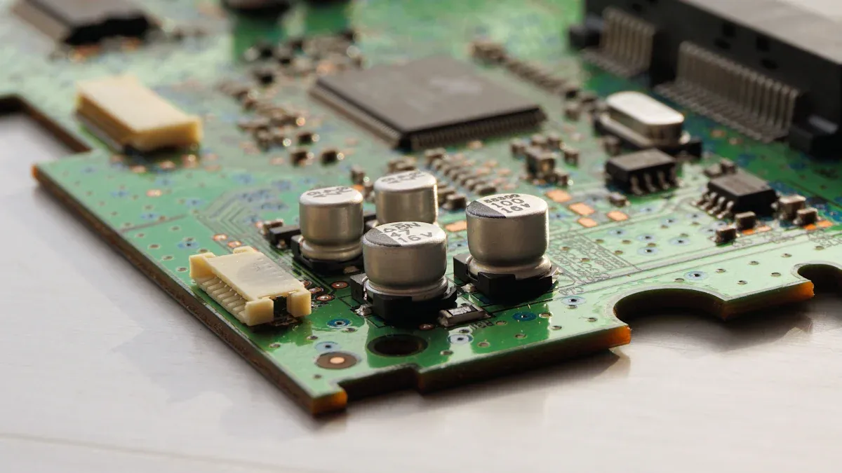
You may wonder what printed circuit board assembly pcba really means. PCBA stands for printed circuit board assembly. This process takes a bare pcb and turns it into a working electronic device by attaching and connecting various electronic components. You will find that a typical pcb contains layers of materials like fiberglass, copper, solder mask, and silkscreen. These layers help organize and protect the electrical paths that connect each part.
The main components you see on a pcb include:
Integrated circuits (ICs)
Resistors
Capacitors
Inductors
Diodes
Transistors
Connectors
Oscillators and resonators
Microcontrollers
Sensors
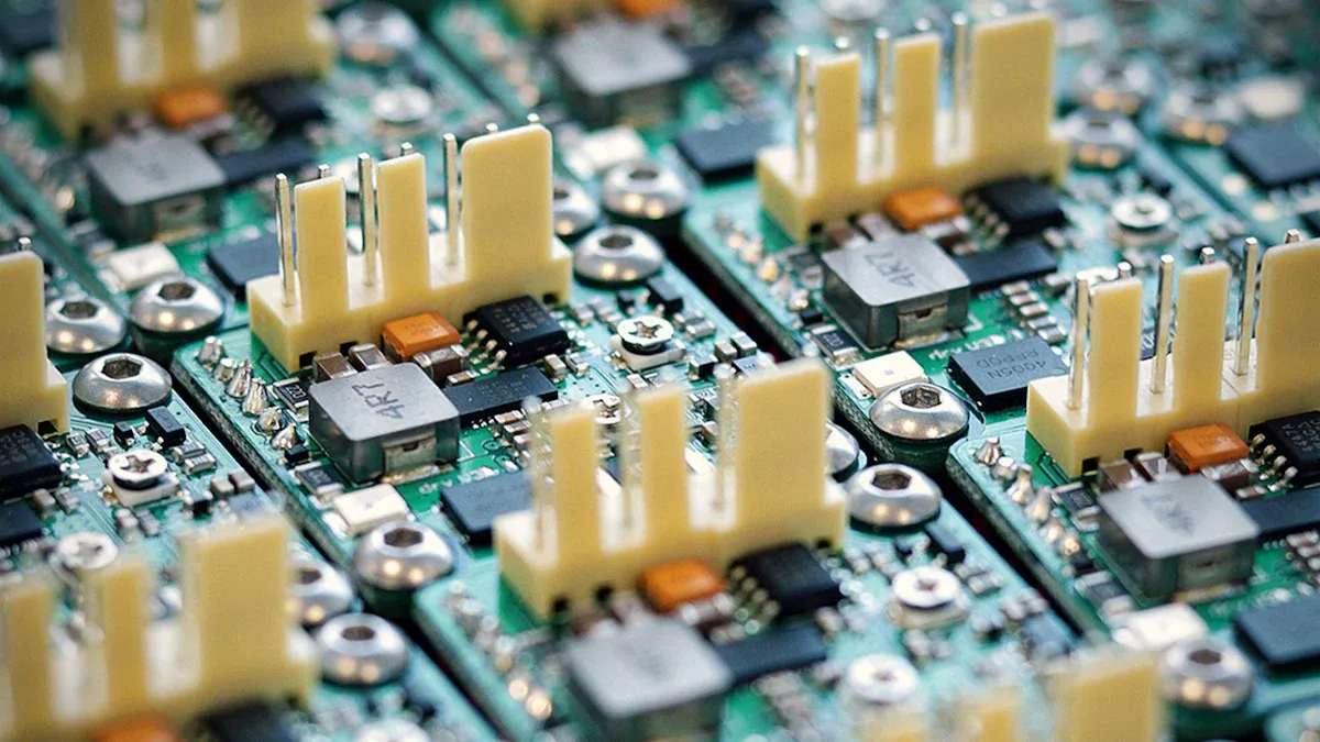
You can use different assembly methods, such as Surface Mount Technology (SMT) and Through-Hole Technology (THT). SMT places components directly onto the surface of the pcb, while THT involves inserting component leads through holes in the board. Some advanced designs use both methods for complex assemblies.
The pcb assembly process follows several key stages recognized by industry standards:
Design and manufacturing of the bare pcb
Preparation of materials and components
Solder paste application using a stencil
Placement of components with pick-and-place machines
Reflow soldering to secure surface-mounted parts
Through-hole component insertion and wave soldering
Inspection and testing, including visual checks, AOI, and X-ray
Cleaning and final packaging
Each step ensures that your pcb assembly meets strict quality and performance requirements.
Why Is the PCB Assembly Process Important?
The pcb assembly process plays a vital role in the reliability and performance of every electronic product you use. If you skip or rush any step, you risk defects that can cause devices to fail or perform poorly. Careful assembly helps prevent issues like poor solder joints, misplaced components, or electrical shorts.
You will notice that the pcb assembly process includes many quality control measures. These steps help catch problems early and ensure that each board works as intended. For example, automated optical inspection (AOI) and X-ray inspection can detect hidden defects that are hard to see with the naked eye. Functional testing checks that the finished product performs its job correctly.
Tip: Always choose a provider that follows international standards and uses advanced inspection tools. This approach gives you peace of mind and helps you avoid costly mistakes.
LTPCBA stands out in the industry for its commitment to quality assurance. The company holds certifications such as ISO 9001, IATF, UL, RoHS, and complies with IPC standards like IPC-A-610 and IPC-6012. LTPCBA uses advanced inspection technologies, including AOI, X-ray, and functional testing, to ensure high precision and reliability. Their automated SMT, BGA, and rigid-flex assembly systems, along with ERP and MES production control, help maintain a high product pass rate of 99.5%. This level of quality supports critical industries such as medical, automotive, and aerospace.
Provider | Certifications | Quality Control Methods | Product Pass Rate | Industry Compliance | Support & Pricing |
|---|---|---|---|---|---|
LTPCBA | ISO 9001, IATF, UL, RoHS, IPC-A-610, IPC-6012 | AOI, X-ray, Functional Testing | 99.5% | Medical, Automotive, Aerospace | 24/7 support, competitive |
PCBWay | ISO 9001, UL, RoHS, IPC-A-610 | AOI, Functional Testing | N/A | IPC standards | Email, chat, phone |
JLCPCB | ISO 9001, UL, RoHS, IPC-A-610 | AOI, Functional Testing | N/A | IPC standards | Email, chat, phone |
You benefit from LTPCBA’s rigorous quality checks at every stage of the pcb assembly process. The company uses advanced tools and highly trained technicians to deliver reliable results. With LTPCBA, you can trust that your printed circuit board assembly pcba will meet the highest standards, whether you are building a prototype or a full production run.
Design and Preparation
PCB Layout and Documentation
You start every successful pcb assembly with a strong design and prototype phase. This step shapes how well your pcb will perform and how easy it will be to manufacture. You need to define the board’s size, function, and environment. Creating a detailed schematic and a bill of materials guides your layout and helps you avoid mistakes later.
When you lay out your pcb, you must follow industry standards like IPC-2221 and IPC-2222. These standards help you improve yield and manufacturability. For example, one company improved its pcb yield from 25% to 88% just by redesigning according to IPC guidelines. You should always check electrical rules and design rules to ensure your pcb meets all requirements. Place components logically, keep similar parts together, and maintain consistent orientation. This makes assembly easier and reduces errors.
You also need to prepare clear documentation. Include hardware drawings, schematics, layout files, and assembly instructions. Add test points and fiducials for inspection. Good documentation speeds up pcb fabrication and assembly. LTPCBA supports you by reviewing your design and documentation, helping you catch issues before production begins.
Tip: Early collaboration with your manufacturer leads to better results. You can solve complex design challenges and avoid costly changes later.
DFA Verification
Design for Assembly (DFA) verification is a key part of the design and prototype process. You check footprints, compare land patterns, and review the bill of materials. You also make sure silkscreen markings are clear and rotation data matches. These checks help you spot problems before pcb fabrication starts.
You should use standard components and avoid complex layouts. This reduces assembly time and errors. DFA verification also means you design for both surface mount and through-hole assembly, keeping pad sizes and spacing uniform. By thinking about assembly early, you prevent delays and lower costs.
LTPCBA offers expert DFA review. Their team checks your pcb design for assembly issues and suggests improvements. This support helps you deliver a reliable product and keeps your project on schedule.
Component Sourcing and Inspection
Ordering Components
You need to source high-quality components for your pcb to ensure reliable performance. Start by choosing authorized and reputable distributors such as Digi-Key, Mouser, and Arrow. These suppliers guarantee authenticity and help you avoid counterfeit parts. You should build strong relationships with your suppliers. This gives you priority service and access to the latest technologies. Always prioritize quality over price. Cheap components can lead to costly problems during pcb fabrication and assembly.
Consider these best practices when ordering components for your pcb:
Diversify your suppliers to reduce supply chain risks.
Maintain buffer stock to handle unexpected shortages.
Require certifications like ISO and IPC from your suppliers.
Use real-time inventory tracking to manage your parts efficiently.
Select suppliers with a proven track record and fast delivery.
LTPCBA supports you with flexible sourcing models. You can choose turnkey solutions, where LTPCBA handles all component procurement, or partial sourcing if you want to supply some parts yourself. LTPCBA’s long-term purchasing service covers over 40,000 parts, ensuring quick access to traceable and authentic components for any pcb project.
Tip: Always verify that your components come with proper documentation and compliance certificates. This step protects your pcb from hidden risks.
Quality Inspection
After you receive your components, you must inspect them before using them in your pcb assembly. Quality inspection helps you catch defects, prevent counterfeit parts, and ensure every component meets industry standards. You should use a combination of visual checks and advanced testing methods.
Common inspection methods include:
Visual inspection for surface defects or irregularities.
X-Ray imaging to analyze internal structures and verify authenticity.
Decapsulation to check internal die markings.
AC/DC functionality tests to confirm electrical performance.
Solderability testing to ensure reliable joints during pcb fabrication.
XRF analysis for material composition and RoHS compliance.
Scanning microscopy for high-resolution surface checks.
Inspection Method | Purpose/Description | Notes/Standards |
|---|---|---|
Visual Inspection | Detect visible defects or irregularities | Basic initial check |
Decapsulation Test | Inspect internal structure and die markings | Counterfeit detection |
AC/DC Functionality Test | Verify operational performance | Electrical conformity |
X-Ray Inspection | Examine internal structure for defects and authenticity | Non-destructive check |
Solderability Testing | Ensure reliable solder joints | J-STD-002B standard |
XRF Test | Analyze material composition for compliance | RoHS verification |
LTPCBA uses strict quality control with 100% authentic parts, third-party validation, and advanced warehouse management. You benefit from incoming inspections, supplier audits, and real-time tracking. These steps ensure your pcb meets the highest standards for performance and reliability.
Solder Paste Application
Stenciling Process
You start the assembly process by applying solder paste to your pcb. This step uses a stencil to deposit the solder paste only on the pads where components will sit. The stenciling process is critical because it controls how much solder paste goes onto each pad. If you use too much or too little, you risk defects like bridging or poor connections.
Several factors influence the accuracy of solder paste application on your pcb:
Solder paste properties, such as viscosity and particle size, affect how well the paste flows through the stencil.
The flatness of your pcb ensures the stencil sits evenly, which helps achieve uniform paste deposits.
Stencil thickness and aperture size determine the volume of solder paste applied to each pad.
Squeegee pressure, speed, and angle control how the solder paste moves across the stencil.
Regular cleaning of the stencil prevents residue buildup, which can clog apertures and cause uneven application.
Operator skill and the production environment also play a role in maintaining consistency.
Tip: Clean your stencil every 5-10 prints to avoid defects and ensure even solder paste coverage on your pcb.
A well-designed stencil improves the consistency of solder paste deposition. You should use apertures slightly smaller than the pad size, usually about 90%, to prevent excess solder paste. Step stencils help when your pcb has mixed component sizes, allowing for precise paste volume across the board.
Solder Paste Quality
The quality of solder paste directly affects the reliability of your pcb assembly. Industry standards like IPC-J-STD-005 and JIS-Z-3284 set strict requirements for solder paste quality. You should look for solder paste that passes tests for viscosity, particle size, metal content, and slumping. These tests ensure the solder paste will print cleanly and form strong joints.
Key tests for solder paste quality include:
Flux residue corrosion testing to check for harmful residues.
Insulation resistance testing to prevent leakage on high-density pcb designs.
Solder joint reliability testing to measure strength and durability.
3D Solder Paste Inspection (SPI) to check the volume, height, and area of each deposit on your pcb.
A table can help you see the main quality checks:
Test Type | Purpose |
|---|---|
Viscosity | Ensures smooth printing |
Particle Size | Prevents clogging and uneven deposits |
Metal Content | Maintains proper solder joint formation |
Slumping | Avoids spreading after printing |
Wetting | Ensures good adhesion to pcb pads |
You should always stir solder paste before use and store it properly to maintain its properties. By following these guidelines, you help ensure your pcb assembly process produces reliable and high-quality results.
SMT Component Placement
Pick and Place Machines
You see pick and place machines at the heart of the smt assembly process. These machines use advanced vision systems and robotic arms to place components on your PCB with incredible precision. Modern pick and place machines achieve tolerances as tight as ±0.01 mm. This level of accuracy ensures that each component sits perfectly on its pad, reducing the risk of soldering defects. You benefit from real-time verification and orientation checks, even when machines operate at speeds of up to 50,000 components per hour. When you improve placement accuracy by just 0.05 mm, you can reduce soldering defects by up to 15%. Calibration plays a key role in maintaining this precision. Technicians align vision systems, nozzles, and feeders using test boards with reference points. Automatic adjustments for nozzle wear help lower errors by 20%. These features allow pick and place machines to balance speed and accuracy, supporting high-volume production while keeping error rates below 0.001%.
Tip: Regular calibration and maintenance of pick and place machines help you achieve consistent results and minimize defects in your smt assembly process.
LTPCBA's SMT Assembly Services
You gain several advantages when you choose LTPCBA for your smt assembly process. The company uses high-end pick and place machines, which are calibrated by experienced technicians. Strict soldering profiles and advanced equipment prevent common defects like solder bridges and cold solder joints. LTPCBA’s quality control system includes incoming inspection, in-line checks after pick and place and soldering, and Automated Optical Inspection (AOI). Final functional testing verifies that your PCB works as intended. Continuous improvement efforts, such as equipment upgrades and staff training, help maintain high yield rates.
Quality Practice / Performance Metric | Impact / LTPCBA Performance |
|---|---|
Reduces rework rates by over 50% | |
Statistical Process Control (SPC) and Defect Trend Analysis | Reduces common defects by 15% |
AI-driven AOI Systems | Reduce downtime by 20% and cut faulty component costs by 30% |
First-pass Yield | 99.5%, significantly above industry average |
Defect Detection Rate | 98.7%, surpassing industry average of 90–95% |
Throughput (Boards per Hour) | 120, exceeding typical 50–100 boards/hour |
False Alarm Rate | Less than 2%, better than industry standard of <5% |
On-Time Delivery Rate | 99%, above industry average of 90–95% |
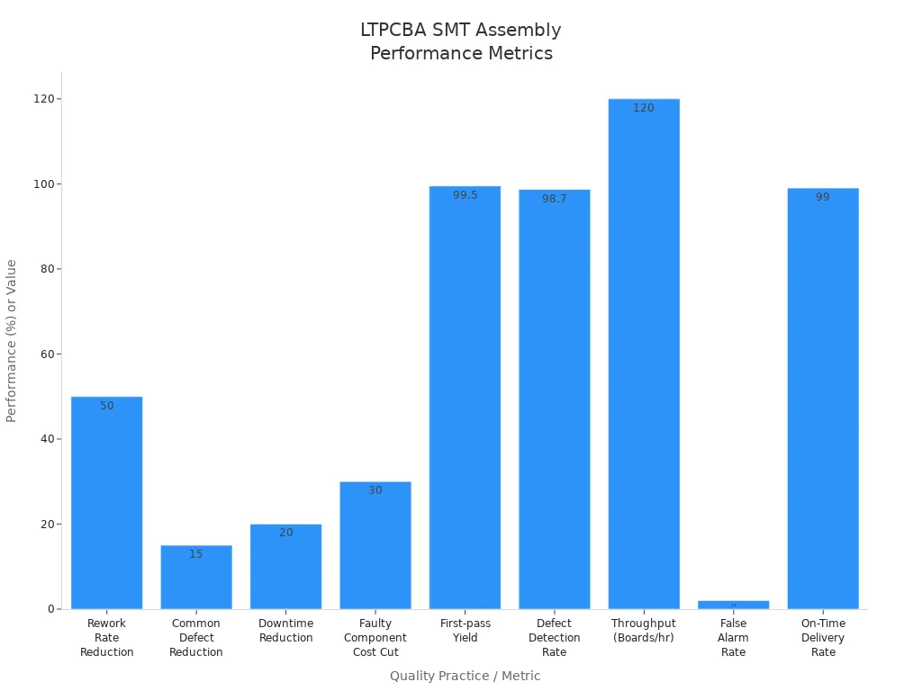
You can trust LTPCBA to deliver high throughput and low defect rates in every smt assembly process. Their commitment to quality and efficiency helps you achieve reliable results for both prototypes and production runs.
Reflow Soldering
Temperature Profile
You control the reflow soldering process by following a precise temperature profile. This profile ensures that solder paste melts and forms strong joints without damaging your components. Each stage in the profile has a specific purpose and temperature range. You can see the typical steps below:
Preheat Zone: Gradually raise the PCB temperature to activate the flux and prevent thermal shock.
Temperature: 25–150°C (leaded), up to 180°C (lead-free)
Duration: 60–90 seconds
Heating Rate: 1.5–3°C/sec
Soak Zone: Hold the temperature steady to activate the flux and equalize heat across the board.
Temperature: 150–200°C (leaded), 180–220°C (lead-free)
Duration: 60–120 seconds
Reflow Zone: Reach the peak temperature to melt the solder and form the joints.
Temperature: 210–240°C (leaded), 240–260°C (lead-free)
Time Above Liquidus: 30–60 seconds
Cooling Zone: Lower the temperature at a controlled rate to solidify the solder joints.
Cooling Rate: 2–4°C/sec
Duration: 30–60 seconds
Reflow Zone | Temperature Range (°C) | Duration (seconds) | Heating/Cooling Rate (°C/sec) | Notes |
|---|---|---|---|---|
Preheating | 25–160 | 60–90 | 1–3 | Activates flux, prevents thermal shock |
Soak (Insulation) | 120–160 | 60–100 | Minimal | Stabilizes temperature, removes oxides, prevents bridging |
Reflow | 210–230 (leaded), 235–250 (lead-free) | 20–30 | N/A | Melts solder, avoid prolonged exposure above 200°C |
Cooling | Ambient to <50 | 30–60 | 3–10 | Rapid cooling forms strong joints, slow cooling causes defects |
Tip: Adjust your temperature profile based on the solder paste datasheet, PCB size, and component sensitivity for best results.
Solder Joint Formation
You create reliable solder joints by controlling both the temperature and the process during reflow. Proper solder joint formation gives your PCB strong mechanical bonds and stable electrical connections. If you use the right temperature and flux, you prevent oxidation and avoid weak joints. You also reduce the risk of defects like bridging, cold joints, or cracks.
A well-formed solder joint improves your PCB’s ability to handle vibration and temperature changes. For example, increasing the pad size within a certain range can boost vibration life by over 30 times. However, you must balance pad size and design for your specific application. Smaller pads help with thermal fatigue, while larger pads work better in high-vibration environments.
You should always inspect solder joints for smooth, shiny surfaces and proper wetting. Avoid dull or cracked joints, as these can fail under stress. Using thermal relief vias and proper spacing helps you achieve uniform heating and strong joints. By following these best practices, you ensure your assembled PCBs remain reliable and durable in real-world conditions.
Through-Hole Assembly
Component Insertion
You use through-hole assembly when you need strong mechanical connections on your PCB. In this process, you insert component leads into holes drilled through the board. You then secure these leads on the opposite side with solder. This method works well for connectors, large capacitors, and components that face physical stress.
You often choose through-hole assembly for prototypes or products that must survive harsh environments. The leads passing through the board give extra strength. You can easily replace or adjust parts during testing. This flexibility helps you when you need to make changes quickly.
Note: Through-hole assembly takes more time than surface mount assembly. You must drill holes and place each component by hand or with machines. This step increases the cost for large production runs, but it gives you higher reliability in tough conditions.
Feature | Through-Hole Assembly (THA) | Surface Mount Assembly (SMA) |
|---|---|---|
Mechanical Strength | Stronger bonding; good for stress and prototyping | Smaller size, higher density, faster mounting |
Cost & Efficiency | More time and cost due to drilling and manual work | Lower cost, faster, no drilling needed |
Reliability | Best for mechanical stress | Reliable in stable settings, less so under stress |
Wave Soldering
After you insert the components, you use wave soldering to attach them to the PCB. You place the board on a conveyor belt that moves it over a wave of molten solder. The solder touches the exposed metal leads and pads, creating strong electrical and mechanical bonds.
Wave soldering works best for boards with many through-hole parts. It gives you consistent results and speeds up the process compared to hand soldering. You must make sure the board is clean and the components are secure before soldering.
You get strong joints that handle vibration and heat.
You reduce the chance of cold or weak solder joints.
You improve the durability of your finished product.
Tip: Use wave soldering for products that need to last in tough environments, such as automotive or industrial electronics. This method helps you achieve high reliability and long service life.
Inspection and Testing in PCB Assembly
Visual and AOI Inspection
You need to check every PCB carefully before it leaves the factory. Visual inspection is your first line of defense. You look for problems like solder bridges, component misalignment, and polarity reversal. You also check for pad lifting, microcracks, and contamination. These issues can cause your board to fail or work poorly.
Automated Optical Inspection (AOI) uses cameras and software to scan each board. AOI finds defects that your eyes might miss, such as:
Solder joint issues like too much or too little solder.
Misaligned or missing components.
Damaged or incorrect parts.
Surface scratches and copper trace problems.
Solder paste defects.
Polarity and rotation errors.
Lifted leads and tombstoning.
AOI works fast and checks every board with high accuracy. You can trust AOI to catch small problems before they become big ones. LTPCBA uses advanced AOI systems and skilled technicians to ensure your boards meet strict quality standards.
Tip: Regular inspection and testing help you avoid costly repairs and keep your products reliable.
Functional Testing
You want to make sure your PCB works as designed. Functional testing checks if the board performs its job in real-world conditions. You connect the board to test equipment and run it through its normal operations. This step finds problems that visual checks or AOI might miss.
You may also use X-ray inspection to look inside solder joints, especially for hidden defects like voids or head-in-pillow issues. In-Circuit Testing (ICT) checks each component and connection for correct values and placement.
LTPCBA combines all these methods—visual checks, AOI, X-ray, ICT, and functional testing—to deliver a 99.5% pass rate. You benefit from their advanced inspection and testing systems, which catch defects early and ensure high-quality results. This complete approach to testing and inspection gives you confidence in every board you receive.
Inspection Method | What It Detects | When Used |
|---|---|---|
Visual | Surface defects, misalignment | Early and final |
AOI | Solder, placement, orientation | In-line, post-solder |
X-ray | Hidden solder issues | After assembly |
ICT | Electrical faults | After assembly |
Functional | Real-world performance | Final stage |
Cleaning and Final Assembly
Cleaning Methods
You must remove flux residues and contaminants from your PCB after assembly. Clean boards help prevent corrosion, electrical shorts, and reliability issues. You can choose from several cleaning methods, each suited to different production volumes and board complexities.
Manual Cleaning: Use soft brushes and lint-free wipes with isopropyl alcohol (IPA) for prototypes or small batches. IPA dissolves rosin and some no-clean flux residues. For stubborn residues, commercial flux removers like MicroCare VeriClean work better and are safer for delicate components.
Ultrasonic Cleaning: High-frequency sound waves in cleaning solutions reach tight spaces and remove residues from complex PCBs. You must control settings to avoid damaging sensitive parts.
Automated Cleaning Systems: Spray-in-air or immersion systems handle high-volume production. These systems use engineered fluids matched to the flux type. You get consistent results and save labor.
Tip: Always match your cleaning agent to the flux type. Use deionized water for water-soluble flux. Test cleaning on small batches before scaling up. Rinse and dry boards thoroughly to prevent moisture-related failures. Wear gloves and ensure good ventilation when handling solvents.
Cleaning Method | Best For | Key Features |
|---|---|---|
Manual Cleaning | Prototypes, small runs | Simple, flexible, uses IPA or VeriClean |
Ultrasonic Cleaning | Complex PCBs | Deep cleaning, controlled settings |
Automated Systems | High-volume production | Consistent, scalable, engineered fluids |
Final Assembly and Packaging
You complete the PCBA process by assembling and packaging your boards. Proper final assembly protects sensitive components from mechanical and thermal stress. You can use reinforcement polymers, such as underfills and edgebonds, to distribute mechanical loads and strengthen solder joints. High-reliability solder pastes improve resistance to thermal fatigue and extend the life of your product.
Material compatibility matters throughout assembly and packaging. You avoid failures like voids, delamination, and die cracking by choosing the right materials for your application. A flexible approach lets you meet space, cost, and performance needs.
You should include inspection points during final assembly. Dual-sided AOI systems detect defects early, such as missing components or soldering issues. Early detection reduces repair costs and improves yield rates. AOI feedback helps you optimize your process and maintain high reliability.
Note: Careful final assembly and packaging maximize the operational lifetime of your PCBA. You deliver products that perform reliably in real-world conditions.
PCBA Manufacturing Process Quality Assurance
International Standards
You need to follow strict international standards to ensure the quality and safety of every pcba. These standards guide the entire pcb assembly process, from design to final inspection. When you choose a manufacturer that meets these requirements, you can trust that your products will perform reliably and safely in any market.
Here are some of the most important international standards for the pcba manufacturing process:
ISO 9001:2015: This standard sets the foundation for a quality management system. It ensures that every step in the pcb assembly process meets consistent quality requirements.
ISO 13485: If you work with medical devices, this standard guarantees that your pcba meets strict regulations for safety and performance.
UL Certification: UL focuses on electrical and fire safety. You need this certification for products sold in North America.
IATF 16949: This standard is essential for automotive electronics. It emphasizes defect prevention and continuous improvement.
RoHS Certification: RoHS ensures that your pcba does not contain hazardous substances restricted by European regulations.
CE Certification: CE shows that your products meet European health, safety, and environmental standards.
IPC Certification: IPC standards cover best practices for pcb design, manufacturing, and assembly.
ISO 14001: This standard demonstrates your commitment to environmentally responsible manufacturing.
Tip: Always check for these certifications when selecting a pcb assembly process partner. They show that the manufacturer follows global best practices and delivers safe, high-quality products.
You will see that these standards not only protect end users but also help you avoid costly recalls and compliance issues. For example, UL certification (such as UL 796) proves that your pcba meets strict safety rules for the US and Canada. ISO 9001 and IATF 16949 show that your manufacturer can deliver consistent quality for demanding industries like automotive and medical electronics.
LTPCBA's Quality Commitment
You benefit from LTPCBA’s strong commitment to quality at every stage of the pcb assembly process. The company holds certifications such as ISO 9001:2015, IATF 16949, UL, and IPC. These certifications prove that LTPCBA meets the highest international standards for both pcb fabrication and assembly.
LTPCBA uses advanced inspection technologies to ensure that every pcba meets strict quality requirements. You will find that their process includes:
3D Automated Optical Inspection (AOI) for precise defect detection.
X-ray inspection to check hidden solder joints and internal connections.
100% visual inspection and mechanical checks based on IPC-600 class II or III.
Electrical Testing (E-Test) to verify circuit continuity and performance.
Functional testing to confirm that each pcba works as intended before shipping.
You can see how LTPCBA’s quality checks cover every stage of the pcb assembly process:
Stage | Critical Quality Checks |
|---|---|
Design Phase | Component selection, PCB layout, ESD protection |
Manufacturing | Surface quality, placement accuracy, soldering control, inline AOI and visual inspections |
Testing | Electrical and functional testing, burn-in, environmental stress tests |
Packaging | Material selection, sealing integrity, temperature and time control |
LTPCBA also tracks and documents every step in the pcba manufacturing process. You get full traceability, which helps you solve problems quickly if they arise. The company uses automation and AI-driven inspection systems to improve accuracy and efficiency. This approach leads to a 99.5% first-pass yield and a 99% on-time delivery rate.
You can trust LTPCBA to deliver reliable results, whether you need prototypes or large production runs. Their dedication to quality assurance means you receive pcba products that meet or exceed industry standards every time.
Note: Quality checks at every stage of the pcb assembly process help you avoid defects, reduce costs, and ensure long-term reliability for your electronic products.
You can achieve reliable electronics by following each step in the pcba process:
Place components accurately.
Solder through-hole parts for strength.
Clean boards to prevent corrosion.
Verify function before deployment.
LTPCBA supports you with advanced inspection tools, fast turnaround, and expert guidance. Start with simple projects like LED blinkers, use quality tools, and learn from tutorials. Stay curious and pay attention to detail as you build your skills.
FAQ
What is the difference between PCB and PCBA?
You see a PCB as a bare board with copper traces and pads. PCBA means the board has all components mounted and soldered. PCBA is ready for use in electronic devices.
How long does the PCBA process take?
You can expect prototype assembly to take 3–7 days. Production runs may take 1–3 weeks. LTPCBA offers fast quotes and on-time delivery for every order.
Why is quality inspection important in PCBA?
Quality inspection helps you catch defects early. You avoid costly repairs and ensure your boards work as designed. LTPCBA uses AOI, X-ray, and functional testing for reliable results.
Can I order small batches or prototypes from LTPCBA?
Yes! You can order small batches or even single prototypes. LTPCBA supports students, hobbyists, and professionals with flexible order sizes and quick turnaround.
See Also
Comprehensive Overview of PCBA Manufacturing Steps for All Levels
Understanding PCBA And Its Essential Parts Explained Clearly
Defining The Meaning Of PCBA In Electronic Systems
PCBA Services Explained From Production Through Final Testing