A Complete Guide to PCBA LED Design and Assembly for 2025

Achieving high reliability in pcba led projects for 2025 demands expertise in pcba led assembly techniques and a thorough understanding of the latest advancements in design and manufacturing. Companies are increasingly adopting automation, high-density interconnects, and sustainable practices to meet the growing performance requirements of pcba led applications. LTPCBA distinguishes itself by consistently delivering top-quality pcba led and led pcb assembly services, backed by state-of-the-art facilities and rigorous quality standards. By implementing proven assembly processes and integrating cutting-edge technologies, teams can ensure their pcba led solutions remain both competitive and dependable.
Trend
Impact on PCBA LED Assembly
Automation
Accelerates pcba led assembly with precision and customization
Sustainability
Promotes eco-friendly pcba led processes and materials
Key Takeaways
Choosing the right materials and substrates, like aluminum or ceramic, improves heat management and extends LED lifespan.
Following design best practices, including proper layout and thermal management, ensures reliable and energy-efficient LED PCBs.
Using advanced assembly methods such as Surface Mount Technology and automated placement increases precision and production speed.
Rigorous quality control with testing and inspection guarantees high performance and reduces defects in LED PCB assemblies.
Embracing automation, advanced materials, and sustainable practices drives innovation and cost savings in LED PCB manufacturing for 2025.
PCBA LED Basics
What is PCBA LED?
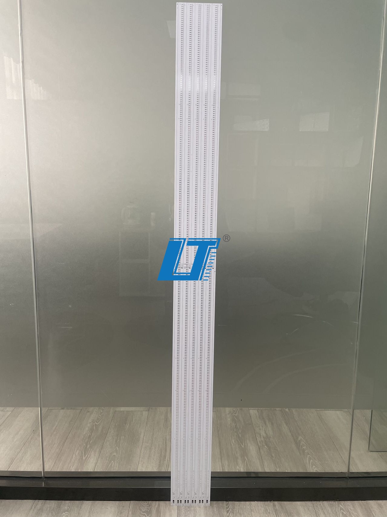
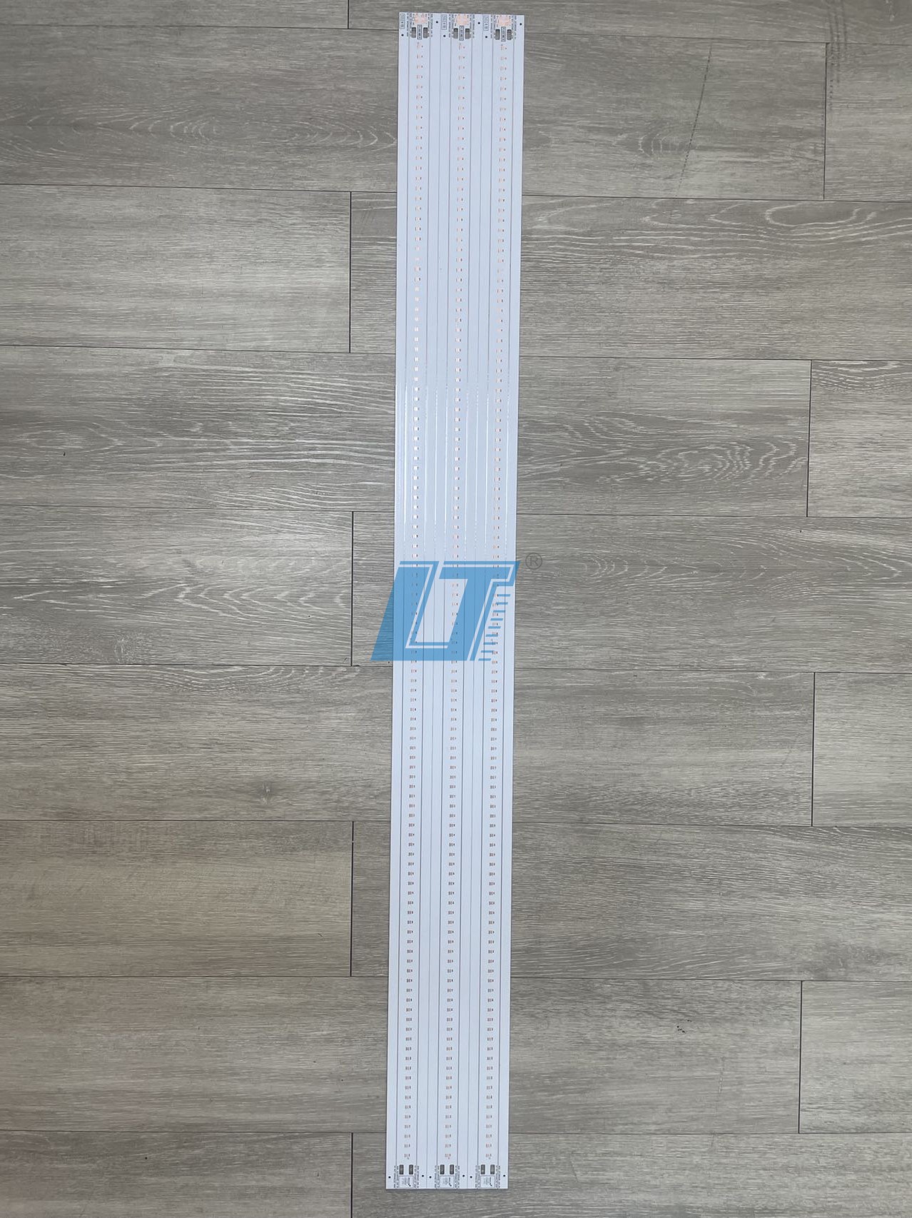
PCBA LED refers to the integration of light-emitting diodes onto printed circuit boards through advanced assembly processes. Engineers use pcba led technology to create efficient lighting solutions for consumer electronics, automotive systems, and industrial equipment. The led pcb design process involves arranging led components on the board to optimize performance and reliability. Manufacturers select materials that support heat dissipation, such as aluminum, to extend the lifespan of led light pcb assemblies. The combination of precise design and robust assembly ensures that led pcbs deliver consistent illumination and energy efficiency.
Key Components
A typical pcba led system relies on several essential components to function effectively. The led circuit boards feature an aluminum alloy base layer, which provides excellent thermal conductivity. This layer supports a thermal insulation layer that protects against heat and mechanical damage. The copper circuit layer serves as the foundation for mounting components. Common elements found on led pcbs include:
LEDs: These are the primary light sources in the system.
Resistors: They regulate current flow and protect the leds.
Capacitors: These components store charge and stabilize the circuit.
Diodes: They ensure unidirectional current and assist with voltage regulation.
Transistors: Used for switching and amplification in led pcb design.
Integrated Circuits (ICs): These manage complex functions such as signal processing.
Assembly methods for led light pcb systems include surface-mount technology, pick-and-place machines, and reflow soldering. These steps guarantee stable operation and effective thermal management.
Types of LED PCBA
Manufacturers use several types of led pcbs to meet diverse application needs. The most common types include:
Aluminum PCB: Preferred for high-power led applications due to superior heat dissipation.
Flexible PCB: Used in curved or dynamic lighting, such as wearables and automotive interiors.
Rigid PCB: Standard choice for traditional led lighting products.
Multilayer PCB: Supports advanced features like dimming and programmability in complex led pcb design projects.
Material selection plays a critical role in led pcb performance. Aluminum pcbs offer excellent thermal management, while FR-4 provides good industrial utility but less heat dissipation. Epoxy pcbs are less common due to their fragility. Engineers choose single-layer led circuit boards for specific applications that require simple structure and reliable operation. Surface mount technology and through-hole technology both contribute to the assembly of led light pcb systems, depending on mechanical and electrical requirements.
Tip: Selecting the right type of led pcb and optimizing the design process ensures long-lasting, high-performance pcba led solutions.
LED PCB Design
Schematic & Layout
Engineers begin every led pcb design project with an initial design and schematic. They follow best practices for efficient design to achieve high performance and reliability. Careful placement of leds ensures uniform light output. Linear rows or symmetrical grids help avoid shadowing and crowding. Adequate spacing between leds supports consistent illumination and energy efficiency.
Designers calculate trace widths based on current requirements. They use trace width calculators and minimize trace lengths to reduce voltage drops. Sufficient spacing between traces and high current planes, at least three times the trace width, provides electrical isolation and improves heat dissipation. Many led pcb designs use four-layer or more boards with full ground and power planes. This approach distributes current and heat evenly across the led pcb.
Thermal management features such as large thermal pads, thermal vias, and thermal relief cutouts enhance heat dissipation. Designers select substrate materials with high thermal conductivity to support led performance. Immersion silver plating improves heat transfer and supports energy efficiency. Thicker copper layers, minimized vias in current paths, and large copper power and ground planes help manage high current loads.
Manufacturing guidelines recommend SMT soldering with heat-sensitive solder paste and nitrogen reflow. Automated optical inspection and in-circuit testing verify the quality of led pcbs. Engineers monitor led voltages and junction temperatures during testing. Thermal imaging and burn-in screening ensure reliability and consistent energy efficiency.
Tip: Following pcb layout guidelines and rigorous inspection protocols leads to reliable led pcb design and long-lasting led pcbs.
Material Selection
Material selection plays a critical role in led pcb design. Engineers evaluate thermal conductivity, dielectric properties, manufacturability, and cost. The table below compares common materials used in led pcb designs:
Material Type | Thermal Conductivity | Dielectric Properties (Constant, Dissipation, Strength) | Manufacturability | Cost Considerations |
|---|---|---|---|---|
FR4 Glass Epoxy | Moderate; glass fiber improves thermal conduction over pure resin | Reasonable dielectric constant and strength; suitable for many LED applications | Highly manufacturable with standard PCB processes; widely used | Most cost-effective; suitable for cost-sensitive applications |
Metal Core PCBs (Aluminum or Copper base) | High thermal conductivity; excellent heat dissipation critical for high-power LEDs | Dielectric layer coating provides electrical insulation | Requires special fabrication equipment; more complex than FR4 | Higher cost than FR4 due to materials and processing complexity |
Ceramic PCBs (Alumina, Aluminum Nitride) | Superior thermal conductivity; best for heat dissipation | Excellent dielectric properties; low losses and high dielectric strength | Manufacturing is complex and costly; specialized processes needed | Highest cost; justified for demanding high-power or high-frequency LED applications |
Thermal conductivity is essential for dissipating heat generated by leds. Dielectric properties affect electrical performance and signal integrity. Manufacturability determines the feasibility and cost of producing led pcbs. FR4 offers the easiest manufacturing process and lowest cost. Metal core and ceramic substrates provide better thermal management but require specialized processes and higher investment. Selecting the right material balances thermal management, electrical performance, manufacturability, and cost to optimize led pcb design and energy efficiency.
Thermal Management
Thermal management remains a cornerstone of led pcb design. Led pcbs must handle high thermal loads to maintain consistent electrical performance and extend the lifespan of leds. Aluminum and other thermally conductive materials serve as common substrates in led pcb designs. These materials effectively dissipate heat and support energy efficiency.
High-performance led pcb assemblies rely on advanced thermal management techniques. Large thermal pads, thermal vias, and relief cutouts help remove heat from critical areas. Applications in automotive, industrial, and residential lighting demand robust thermal management for durability and reliability. Led pcb designs enable energy-efficient lighting by reducing heat generation compared to traditional bulbs. This approach contributes to longer-lasting and eco-friendly solutions.
Aluminum substrates remain a foundational choice for thermal management in led pcb design. Led pcbs support advanced lighting features such as dimming, sensors, and color-changing. Reliable thermal management ensures these features operate without performance loss.
Note: Effective thermal management in led pcb design directly impacts energy efficiency and product longevity.
Design for Manufacturability
Design for manufacturability (DFM) ensures that led pcb designs align with manufacturing capabilities. Engineers apply guidelines to prevent issues such as short circuits, warping, misaligned drill holes, and soldering defects. Key DFM principles include minimum trace width and spacing, correct hole sizes and pad diameters, optimized component placement and orientation, balanced copper distribution, and proper solder mask design.
These guidelines lead to smoother fabrication and assembly. They reduce rework, scrap, and delays, improving production efficiency and yield. Early involvement of manufacturing experts and use of DFM tools help identify and resolve manufacturability issues before production begins.
For led pcb designs, precise assembly and thermal management are critical. DFM ensures reliable solder joints and effective heat dissipation, directly enhancing yield and efficiency. Adhering to design rules and guidelines specific to manufacturing processes minimizes risks of defects and improves overall product quality.
Optimized component selection and placement facilitate automated assembly and testing. This approach increases production throughput and reduces costs. Incorporating design for testability features aids in troubleshooting and quality assurance during manufacturing. Maintaining communication with manufacturers throughout the design and production process ensures continuous alignment with manufacturing capabilities and constraints.
Callout: Applying DFM guidelines in led pcb design supports high yield, efficient production, and consistent energy efficiency.
LED PCB Manufacturing Process
Substrate Selection
Selecting the right substrate is the foundation of successful led pcb assembly. Engineers choose materials based on thermal conductivity, durability, and cost. Aluminum stands out as the most popular choice for led pcb manufacturing. It offers excellent thermal conductivity, supports high led densities, and resists deformation at high temperatures. Aluminum substrates extend the life of led chips in high-power applications. They also support environmental sustainability because aluminum is abundant, recyclable, and non-toxic.
Copper substrates provide even better heat dissipation than aluminum. They suit high-power led applications but increase cost and manufacturing complexity. FR-4 is lightweight and inexpensive. It works well for low-power led pcb assembly where heat dissipation is less critical. Ceramic substrates, such as aluminum nitride and aluminum oxide, deliver superior thermal conductivity and electrical insulation. These materials perform reliably in industrial and automotive lighting.
Flexible substrates use polyimide or polyester. They allow creative designs for curved or decorative lighting. Hybrid substrates combine aluminum with non-thermally conductive materials to balance cost and performance. Epoxy resin offers a budget-friendly option for applications that do not require high strength.
Advantages | |
|---|---|
Aluminum | Excellent thermal conductivity, cost-effective, durable, impact resistant, recyclable, non-toxic, dimensionally stable, resists deformation at high temperatures, supports high led densities and longer runtimes. |
Copper | Superior thermal conductivity, better heat dissipation, suitable for high-power leds, higher cost and complexity. |
FR-4 | Lightweight, inexpensive, good flame retardant properties, suitable for low-power led pcb assembly. |
Ceramic | Excellent thermal conductivity and insulation, durable, ideal for high-power and high-temperature environments. |
Flexible | Design flexibility for curved shapes, used in led strips and decorative lighting. |
Hybrid | Balances cost, rigidity, and thermal performance. |
Epoxy Resin | Low cost, less durable, used in budget-sensitive applications. |
LTPCBA leverages advanced substrate selection to optimize led pcb assembly for each application. Their expertise ensures that every led pcb assembly manufacturer decision supports performance, reliability, and sustainability.
SMT & Assembly
Surface Mount Technology (SMT) drives precision and efficiency in led pcb assembly. The process begins with PCB design and prototyping. Engineers verify prototypes to ensure optimal led placement and circuit integrity. Component sourcing follows, with a focus on high-quality leds, resistors, and capacitors. This step guarantees long-term performance and reliability.
Solder paste application uses stainless-steel stencils to deposit paste onto PCB pads. Inspection confirms correct placement before moving to automated pick-and-place machines. These machines position led components with high accuracy, following pre-programmed coordinates. Reflow soldering secures components by melting the solder paste in a controlled oven. Vapor-phase soldering may be used for sensitive components.
After soldering, automated optical inspection (AOI) checks component placement and solder quality. Engineers perform functional testing to verify that each led pcb assembly meets design specifications. LTPCBA’s advanced SMT lines and automated systems enable high-speed, high-precision led pcb assembly. Their process supports both prototype and mid-volume production runs.
Key Steps in SMT & Assembly
1. PCB Design and Prototyping 2. Component Sourcing 3. Solder Paste Application 4. Pick and Place 5. Reflow Soldering 6. Inspection and Testing
LTPCBA’s commitment to quality and efficiency makes them a preferred led pcb assembly manufacturer. Their quick response and technical support ensure smooth production and on-time delivery.
Quality Control
Quality control is essential for reliable led pcb assembly. LTPCBA implements rigorous measures at every stage of the led pcb manufacturing process. Electrical testing and continuity checks confirm that all connections function correctly. Thermal cycling and stress testing simulate real-world conditions to identify potential failure points.
Soldering quality control involves monitoring temperatures and inspecting joints to prevent defects. Automated systems such as AOI and X-ray inspection verify precise component placement and detect hidden flaws. Functional and burn-in testing expose latent defects by simulating prolonged operation.
Conformal coating protects the finished led pcb assembly from moisture, dust, and other environmental hazards. Adherence to international standards, including ISO 9001 and IPC-2221, ensures consistent quality management and compliance. LTPCBA’s advanced inspection techniques and strict process controls contribute to their 99.5% pass rate in product delivery.
Tip: Choosing a reliable led pcb assembly manufacturer like LTPCBA guarantees efficient production, high-quality results, and long-term reliability for every led pcb assembly project.
LTPCBA’s expertise in led pcb manufacturing, advanced automation, and comprehensive quality assurance practices set them apart in the industry. Their focus on innovation and customer satisfaction supports successful led pcb assembly for diverse applications.
LED PCB Assembly
Surface Mount Technology
Surface mount technology (SMT) has transformed led pcb assembly by enabling higher efficiency and reliability. Engineers use SMT to mount smd led and other components directly onto the surface of the pcb. This approach allows for greater component density, which supports miniaturization and lighter assemblies. SMT enables both sides of the pcb to be populated, increasing design flexibility for led applications.
Key benefits of SMT in led pcb assembly include:
Higher component density, allowing more leds and circuitry in compact spaces.
Smaller, lighter assemblies, ideal for portable led devices.
Highly automatable assembly process, reducing manual labor and errors.
Enhanced reliability of solder joints, especially under thermal and vibration stress.
Lower production costs for high-volume led pcb assembly projects.
SMT also improves electrical performance by reducing lead inductance and resistance, which is important for high-frequency led circuits. These advantages make SMT the foundation of modern one-stop led pcb assembly services.
Automated Placement
Automated placement systems play a critical role in the led pcb assembly process. These machines use advanced vision alignment and high-precision motors to achieve micron-level accuracy. Automated placement reduces human error and ensures consistent quality, which is essential for complex led assemblies.
Feature | Description |
|---|---|
Placement Accuracy | ±0.03mm precision with vision-on-the-fly alignment |
Placement Speed | Up to 40,000 components per hour for led pcb assembly |
Technology | Magnetic levitation motors and precision ball screws for repeatable results |
Automated placement allows thousands of smd led and other components to be mounted quickly and accurately. This speed and precision increase throughput and support the demands of one-stop led pcb assembly. Automated systems operate continuously, making them ideal for high-volume pcb assembly and reducing lead times for led projects.
Soldering & Inspection
Soldering forms the backbone of the led pcb assembly process. Reflow soldering is the most common technique for smd led and other surface-mounted components. Engineers use controlled ovens to melt solder paste, creating strong electrical and mechanical bonds. For through-hole components, wave soldering may be used.
Inspection ensures the quality and reliability of every led pcb assembly. Automated optical inspection (AOI) checks for correct component placement and solder joint quality. X-ray inspection provides a detailed view of solder joints beneath dense packages, revealing hidden defects that AOI cannot detect. Visual inspection under magnification remains important for identifying surface issues during the assembly process. In-circuit and functional testing further verify that each led pcb assembly meets performance standards.
Tip: Combining advanced soldering techniques with thorough inspection ensures every one-stop led pcb assembly delivers long-lasting performance and reliability.
Testing & Troubleshooting
Prototyping
Engineers rely on robust prototyping methods to validate LED PCB designs before mass production. The process begins with EVT (Engineering Validation Test) samples. Teams fabricate multiple prototype PCBs, usually between 5 and 25 units, using production-level processes and the final bill of materials. This approach ensures design consistency and manufacturing compatibility.
Fabricate EVT samples with production processes and final components.
Conduct comprehensive tests, including functional, electrical, and environmental assessments.
Perform vibration testing, such as sinusoidal and random vibration, to check mechanical robustness.
Address mechanical failure modes like solder joint fatigue, component detachment, and PCB deformation by applying proper materials and reinforcements.
Iterate the design based on test results before moving to further validation stages.
These steps in led pcb prototyping and testing help engineers identify and resolve issues early, reducing the risk of costly errors during full-scale manufacturing.
Functional Testing
Functional testing verifies that each LED PCB meets performance and reliability standards. Engineers use a variety of procedures to simulate real-world conditions and detect potential faults.
Description and Purpose | |
|---|---|
Voltage Meter Testing | Measures voltage at various points to ensure correct power levels and safe operation of the PCB. |
Load Testing | Assesses PCB performance under stress conditions such as temperature, current, and operating frequency. |
Quality Control (QC) Testing | Verifies PCB meets design specs and industry standards, often including Automated Optical Inspection (AOI). |
In-Circuit Testing (ICT) | Checks component placement and functionality by applying current and measuring voltage at test points. |
Flying Probe Testing | Uses movable probes to test electrical properties without custom fixtures, ideal for prototypes and small runs. |
Solderability Testing | Ensures components can be properly soldered, preventing poor connections and oxidation issues. |
Detects ionic residues and contaminants that could cause corrosion or failure. | |
Micro-Sectioning Analysis | Examines internal PCB structure for defects like shorts or opens. |
Time-Domain Reflectometer (TDR) | Locates faults in transmission lines by detecting impedance mismatches. |
Peel Testing | Measures adhesion strength of laminate to substrate. |
Solder Float Testing | Tests thermal stress resistance of PCB holes under extreme temperatures. |
Tip: Combining multiple testing methods ensures comprehensive validation and long-term reliability for every LED PCB.
Common Issues
During LED PCB testing, engineers often encounter several recurring problems:
Voltage drops and power supply errors, especially when driving LEDs with PWM signals at certain duty cycles.
Physical damage from impacts, heat, moisture, or corrosion.
Component failures due to wear, poor design, or manufacturing defects.
Soldering issues, such as cold joints or misalignment.
Design flaws, including incorrect routing, poor grounding, and inadequate power distribution.
Environmental factors, like extreme temperatures, that affect component performance.
Lack of ESD protection, leading to damaged sensitive components.
Engineers address these issues by adjusting design parameters, improving component selection, and refining manufacturing processes. Careful troubleshooting and continuous improvement help maintain high standards in LED PCB production.
Cost & Supplier Selection
Cost Drivers
LED PCB design and assembly costs depend on several key factors. Material choice, such as aluminum core substrates, impacts expenses due to thermal management requirements. Board complexity, including layer count and size, increases lamination and drilling costs. Specialized manufacturing processes, like ENIG finishes or microvias, add to the budget. Component types and quantities influence sourcing and assembly costs. Production volume affects per-unit pricing, with larger runs benefiting from economies of scale. Labor rates and automation levels also play a role, as do regional variations—manufacturing in Asia often reduces costs by 10-20%. Rush orders and higher inspection levels raise expenses. Additional steps, such as conformal coating, extend assembly time and cost.
Tip: Simplifying designs, choosing cost-effective materials, and leveraging automation help control LED PCB project budgets.
Choosing LTPCBA
Selecting LTPCBA as a supplier offers distinct advantages for LED PCB projects. Their 99.5% pass rate demonstrates a strong commitment to quality, minimizing errors and reducing costly rework. Customers benefit from LTPCBA’s quick response, with quotations delivered in 2-3 working days and 24/7 technical support. These features enable teams to meet tight deadlines and avoid delays. LTPCBA’s advanced automation and smart machines ensure consistent quality and competitive pricing. Their transparent processes and reliable support make them a cost-effective choice for professionals and small businesses. By partnering with LTPCBA, customers save money, accelerate project timelines, and improve satisfaction.
Callout: LTPCBA’s speed, reliability, and high-quality standards help customers achieve efficient, cost-effective LED PCB assembly.
Compliance & Standards
Compliance with industry standards ensures safety, reliability, and market access for LED PCB assemblies. LTPCBA adheres to ISO 9001, which requires documented procedures and consistent production quality. Automated Optical Inspection (AOI) and In-Circuit Testing (ICT) reduce defects and support rigorous quality control. IATF 16949 addresses automotive requirements, focusing on defect prevention and process control. UL standards, such as UL 94V-0, guarantee fire safety for PCBs. RoHS and REACH regulations restrict hazardous substances, promoting environmental responsibility. These certifications demonstrate LTPCBA’s commitment to quality, safety, and regulatory compliance in every LED PCB project.
Note: Working with a supplier who meets ISO, IATF, UL, RoHS, and REACH standards ensures reliable, safe, and compliant LED PCB assemblies.
Trends for 2025
Automation
Automation shapes the future of LED PCB manufacturing in 2025. Companies now use smart manufacturing systems powered by AI and IoT. These systems automate production lines and monitor processes in real time. Automated lines improve efficiency and reduce the need for manual labor. Smart monitoring detects issues early and helps maintain high product quality. Real-time data allows for quick process adjustments, which leads to fewer errors and higher precision. As a result, manufacturers see lower costs and better consistency in every led project.
Note: Automation and smart technologies drive the latest innovations in LED PCB assembly, making production faster and more reliable.
AI and IoT enable automated production lines and smart monitoring.
Real-time monitoring supports process optimization.
Automation reduces human intervention and improves product quality.
Cost reduction and higher precision benefit all stages of manufacturing.
Advanced Materials
The use of advanced materials marks a major shift in LED PCB design. Flexible substrates like polyimide and PET allow engineers to create thin, lightweight, and bendable led boards. These materials provide excellent thermal stability and dielectric insulation. Copper foil in various thicknesses supports efficient circuitry. Protective coatings such as solder masks and silicone improve durability and shield against moisture and dust. Metal core PCBs with aluminum substrates offer superior heat dissipation, which extends the lifespan of leds. Transparent PCBs made from glass or special polymers allow light to pass through, supporting new design possibilities.
Flexible substrates enable bending and folding without damaging copper traces.
Lightweight, thin boards fit into portable and wearable devices.
Advanced coatings protect against harsh environments.
Metal core PCBs manage heat better than traditional materials.
Transparent and 3D printed PCBs support creative applications.
These advances in led pcb technology open doors to wearable devices, automotive lighting, and smart city infrastructure.
Sustainability
Sustainability stands at the center of modern LED PCB manufacturing. Companies adopt eco-friendly practices to reduce environmental impact. They use low-impact surface finishes and source lead-free, halogen-free materials. Closed-loop wastewater systems recycle and treat water, preventing pollution. Safer etching and plating solutions, such as alkaline etching, replace hazardous chemicals. Manufacturers design PCBs for easy disassembly, making recycling simpler. Responsible recycling partners help manage end-of-life disposal. Compliance with RoHS and REACH ensures safer products and processes.
Automated chemical handling improves safety.
Take-back programs and local recycling centers manage e-waste.
Energy-conscious production methods lower the carbon footprint.
Full lifecycle sustainability guides every step, from sourcing to disposal.
Tip: Sustainable manufacturing not only protects the environment but also supports long-term business success.
Successful PCBA LED projects in 2025 require a focus on best practices and continuous improvement. Key steps include:
Optimize thermal management and signal integrity.
Foster collaboration between design and manufacturing teams.
Common challenges, such as component alignment and thermal issues, can be overcome with automation and careful planning. LTPCBA’s expertise and commitment to quality help teams achieve reliable results. Staying informed about new trends ensures ongoing success in every project.
FAQ
What is the main advantage of using LTPCBA for LED PCB assembly?
LTPCBA offers advanced automation, a 99.5% pass rate, and fast response times. Customers receive high-quality products, reliable support, and efficient project delivery. The company’s expertise ensures consistent results for both prototypes and production runs.
How does LTPCBA ensure quality in LED PCB projects?
LTPCBA uses automated optical inspection, X-ray analysis, and functional testing. The team follows ISO, IATF, and UL standards. These practices guarantee each LED PCB meets strict quality and safety requirements.
Which materials work best for high-power LED PCBs?
Aluminum and ceramic substrates provide excellent thermal management. These materials help dissipate heat quickly, which extends LED lifespan and improves performance. LTPCBA recommends these options for demanding applications.
Can LTPCBA handle both small and large production runs?
Yes. LTPCBA supports prototype batches and mid-volume production. The company’s flexible manufacturing systems adapt to different order sizes, ensuring timely delivery and consistent quality.
What certifications does LTPCBA hold for LED PCB assembly?
LTPCBA holds ISO 9001, IATF 16949, and UL certifications. These standards confirm the company’s commitment to quality, safety, and regulatory compliance in every project.
Tip: For more details or custom requirements, visit LTPCBA’s official website.
See Also
Comprehensive Overview of PCBA Production Steps for All Levels
Essential Tips for Sourcing BOM in PCBA Projects
How to Procure Electronic Parts for PCBA Assembly
Understanding PCBA and Its Key Component Parts
Step-By-Step Instructions for Industrial Controller PCB Design