PCBA Guide and Best Practices for 2026
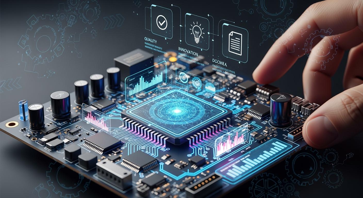
You use a PCBA guide to help build and check electronic boards. PCBA means Printed Circuit Board Assembly. PCB means printed circuit board. You see PCBA in almost every device today, like phones and cars. Best practices in your pcba guide help your designs work well. They make your boards last longer and follow rules in 2026. When you use a pcba guide, you follow smart steps. These steps include DFM analysis, quality checks, and clear paperwork. These steps cut costs and make boards more reliable, as shown below:
Practice | Benefit |
|---|---|
DFM Analysis | Finds problems early and saves up to $170,000 a year. |
Documentation | Reduces mistakes and saves money. |
Quality Assurance | Increases reliability and meets industry standards. |
You get better results when you know your pcba guide. You should understand board types and keep up with design and care.
Key Takeaways
Know the difference between PCB and PCBA. A PCB is only a board. A PCBA is a board with parts on it. It works in devices.
Use best practices like DFM analysis and quality checks. These steps help you save money. They make your boards more reliable.
Pick the right PCB type for your project. Think about flexibility and thermal performance. Also, consider what your project needs. This helps your project succeed.
Keep your PCBA clean and maintained. Clean it often to stop problems like short circuits. Cleaning also stops corrosion. This helps your devices last longer.
Test your PCBA before you ship it. Functional testing makes sure your board works right. It also checks if your board meets quality standards.
PCBA Guide: Process Steps
What Is PCBA
You start with a printed circuit board, which is a flat board that connects electronic parts. When you add chips, resistors, capacitors, and connectors to the board, you create a PCBA. This means you turn a simple pcb into a working part of a device. The pcb design process helps you plan where each part goes. You use the pcb design process to make sure every component fits and works together. In modern electronics, a PCBA is the finished board that powers your phone, car, or computer. The pcb design process gives you a map for placing each part. You need this map before you begin pcb manufacturing.
You should know the difference between a pcb and a PCBA:
A pcb connects circuits but does not work by itself.
A PCBA has all the parts attached and can do its job in a device.
The pcb acts as the base, while the PCBA is the finished product that works.
Key PCBA Stages
You follow several steps in the pcb design process and pcb manufacturing to build a reliable PCBA. Each stage has important tasks. You must pay attention to every detail to avoid problems later.
Stage | Tasks |
|---|---|
Component Placement | You use machines to place each part in the right spot. You check the direction and position. |
You join parts to the pcb using heat. You can use wave, hand, or reflow soldering. | |
Functional Testing | You test the board to make sure it works. You use stress tests to check for weak spots. |
You may face challenges at each stage. Here are some common problems:
Stage | Common Challenges |
|---|---|
Soldering Quality | Weak connections, cold joints, or bridges can cause the device to fail. |
Component Placement | Placing parts in the wrong spot can lead to short circuits or failures. |
Functional Testing | You must find defects by testing how the board works under stress. |
You use the pcb design process to plan for these steps. You use pcb manufacturing to build the board. You check your work at every stage. You use tools like in-circuit testing to measure voltage and current. You use time-domain reflectometry to check the paths on the pcb. You use thermal shock testing to see how the board handles heat and cold. You use highly accelerated life testing to find weak points. You use burn-in testing to make sure the board works when you first turn it on. You use environmental testing to see how the board handles moisture and shaking. You use manual functional testing with tools like multimeters. You use fault simulation to find problems before you build the board. You use adapted cable testing to check how cables work with the pcb.
Why Best Practices Matter
You need best practices in the pcb design process and pcb manufacturing to make sure your boards last and work safely. You must follow strict rules, especially in industries like cars.
In the automotive industry, a single PCBA failure can cause recalls, warranty issues, and even safety incidents. That is why automotive PCBA quality standards are much stricter than in many other markets. OEMs expect 'zero-defect' thinking, full traceability, and strong process control from their PCBA manufacturers.
You must make sure your pcb can:
Withstand extreme temperature cycles.
Tolerate vibration and shock.
Resist corrosion from the environment.
Keep signal integrity for fast communication.
Work safely for 10 years or more.
You use the pcb design process to plan for these needs. You use pcb manufacturing to build boards that meet these high standards. You check your work at every step. You keep records so you can trace every board. You use best practices to avoid mistakes and keep your boards safe and reliable.
PCB Types & Applications
Common PCB Types
You will find that each printed circuit board is custom made for its job. In 2026, you see many types of pcb in electronics. Here are the most common types you will use:
Single-sided pcb
Double-sided pcb
Multilayer pcb
Rigid pcb
Flexible pcb
Rigid-flex pcb
High-density interconnect (HDI) pcb
Each pcb type has a special use. Rigid pcb works best in stable places. Flexible pcb fits in devices that move or bend. HDI pcb helps when you need small size and complex circuits.
Choosing the Right PCB
You need to pick the right pcb for your project. You should look at important features before you decide. The table below shows what you should check:
Criteria | Description |
|---|---|
Electrical Properties | Check if the pcb can handle the signals you need. |
Thermal Performance | Make sure the pcb can handle the heat in your device. |
Mechanical Strength | Decide if you need a pcb that bends or stays stiff. |
Cost and Availability | Balance how much you want to spend with how easy it is to get the pcb. |
Application Needs | Think about rules for your industry, like cars or healthcare. |
Tip: Always match the pcb to your device’s needs. This helps your design last longer and work better.
Application Scenarios
You use different pcb types for different jobs. The table below shows where you might use each pcb:
PCB Type | Key Features & Differences | Typical Applications |
|---|---|---|
Single-layer | Simple, cheap, easy to build | Calculators, cameras, radios |
Double-layer | More parts, both sides used | Power supplies, LED lighting |
Multi-layer | Small, fits lots of circuits | Medical, GPS, data storage |
Rigid | Hard, flat, does not bend | Motherboards, fixed devices |
Flexible | Bends, fits small spaces, costs more | Wearables, compact electronics |
Rigid-flex | Mix of rigid and flexible, for tricky designs | Aerospace, advanced equipment |
You can see that the right pcb helps your device work well in its environment. You should always choose the pcb that fits your project best.
PCB Design Principles
Component Placement
When you design a pcb, you plan where each part goes. Good placement helps your board work better and last longer. You want your pcb layout to make routing easy and keep signals clear. Here are some tips you should use:
Put parts close together for short, direct routes.
Keep related parts in groups to lower noise.
Place sensitive parts away from loud or high-power spots.
Follow the rules for track width, spacing, and clearance.
Make your pcb layout small but keep good signal flow.
Think about heat and put hot parts where they can cool.
Arrange parts so machines can place them easily.
If you use these steps, your pcb is easier to build and works better.
Trace Routing & Signal Integrity
You must route traces with care in your pcb layout. How you route traces changes how signals move through your pcb. If you do not plan, you may get crosstalk or lose signals. The table below shows how routing choices affect signal integrity in your pcb design:
Aspect | Impact on Signal Integrity |
|---|---|
Impedance Control | Traces too close to the edge can change impedance and cause signal problems. |
Crosstalk | Traces close together can cause unwanted signals. More space helps stop this. |
Electromagnetic Interference | Routing over split planes can break return paths and cause signal distortion. |
Keep traces 10–15 mil from the edge of your pcb layout. This helps stop electromagnetic interference and keeps signals clean.
High-Speed PCB Design
High-speed pcb design brings new problems to solve. Fast signals need special care in your pcb layout. Use these ideas to keep your pcb design strong:
Use differential pair routing to block noise.
Build your pcb layout with good layer stackup to cut losses.
Make trace spacing bigger to lower crosstalk and noise.
Add ground planes under signal layers for shielding.
Route important signals on different layers to keep them apart.
Match impedance to stop signal reflections.
Use termination resistors at the end of lines to absorb signals.
Make connectors and vias better to keep signals smooth.
Check your pcb layout for these things before you finish your pcb design. This helps you avoid problems and makes your high-speed pcb design ready for the future.
PCB Design Guides & Documentation
Using PCB Design Guides
You need good pcb design guides to make strong boards. These guides give you rules and tips for each step. If you follow them, you make fewer mistakes. Your pcb will work well in any device. In 2026, engineers use many guides to plan and build each pcb. The table below lists some trusted pcb design guides you can use:
Guide Title | Description |
|---|---|
EMI and EMC Design Guidelines for PCBs | Helps you understand EMI, its sources, and how to reduce interference. |
IPC Standards Handbook | Gives you the main standards for pcb design and quality. |
High-Speed PCB Design Guide | Shows you how to design pcb for fast signals and high-speed needs. |
Design for Manufacturing Handbook | Teaches you how to make your pcb easy to build and cost-effective. |
Pick the right guide for your project. Each guide helps you fix different problems in pcb design. When you use these guides, your printed circuit board is safer and works better.
Documentation & Revision Control
You must keep good records for every pcb design. Clear documentation helps you and your team stay organized. You can track changes and share updates with everyone. Here are some ways strong documentation and revision control help your pcb projects:
Centralized documentation keeps all pcb design files in one place.
Version control lets you track changes and always use the latest files.
Real-time collaboration helps your team work together and fix mistakes quickly.
Standard templates make your pcb design documents clear and easy to read.
Compliance tracking helps you meet industry rules and find important files fast.
Cloud storage lets you access your pcb design from anywhere.
Security settings protect your pcb information from unwanted changes.
When you use these tools, your pcb design process is smooth and safe. You can find problems early and fix them before they get worse. Good documentation and revision control help you finish your pcb projects on time and with fewer mistakes.
Material Selection & Sourcing
Reliable Materials for 2026
You have to pick the right materials for your pcb. This helps your boards last longer and work well. In 2026, you can choose from many options. Some materials are better for certain jobs:
FR-4 multilayer boards are good for control and infotainment systems.
High-TG and high-temperature materials work in engines and powertrains.
Heavy-copper pcbs are used in electric vehicles and power electronics.
HDI pcbs are great for radar, camera modules, and small spaces.
Rigid-flex pcbs fit into small modules and 3D packaging.
Polyimide gives strong heat and chemical resistance.
Rogers and PTFE are best for high-frequency RF and microwave circuits.
Metal core pcbs, like aluminum or copper-backed boards, help cool power electronics or LEDs.
You need to match the material to your device’s needs. This helps your printed circuit board handle stress and last longer.
Supplier Evaluation
You must choose suppliers who give you good pcb materials. Use the table below to compare suppliers:
Evaluation Criteria | Description |
|---|---|
Manufacturing Technology and Production Capability | Check if the supplier can make your pcb design, including layer count and trace width. |
Quality Certifications and Compliance Infrastructure | Make sure the supplier has certifications like IPC-6013 and ISO 9001. |
Engineering Support and DFM Engagement | See if the supplier offers design support and manufacturability reviews. |
Supply Chain Stability and Lead Time Integrity | Look at the supplier’s delivery history and inventory management. |
You should always ask for samples and test them before picking a supplier.
Compliance Considerations
You must follow strict rules when picking pcb materials. These rules keep your boards safe and legal. The table below shows the main compliance types you need to know:
Compliance Type | Key Considerations |
|---|---|
RoHS | Limits hazardous substances. You need lead-free finishes and halogen-free laminates. Material declarations must confirm safe levels. |
REACH | Covers more hazardous substances. You must register and check chemicals used in production. Material qualification helps avoid delays. |
You will face new problems in 2026. AI infrastructure and data centers need more pcb materials. Global supply chains are under more pressure, which can slow down deliveries. You need to plan your material choices carefully to avoid shortages and delays.
Manufacturing Best Practices
DFM Principles
You should use Design for Manufacturability (DFM) principles. This makes your pcb easy to build and helps it work well. DFM helps you stop mistakes and saves time when making boards. You need to talk to your manufacturer early in the design. Share your files and check if your pcb matches what the factory can do. The table below lists the main DFM principles you should follow:
DFM Principle | Description |
|---|---|
Follow design rules | Use the right trace width, clearance, pad size, and via structures. |
Provide access | Leave enough space for inspection and rework, especially near small parts. |
Standardize components | Pick common parts to make assembly and supply easier. |
Consider thermal paths | Plan for heat flow and keep hot parts away from sensitive ones. |
Plan for testing | Add test points and connectors for easy checking. |
Ask your manufacturer for help during design.
Share your files and details early.
Make sure your pcb fits the factory’s trace width and spacing limits.
Quality Control
You need strong quality control to make sure your pcb works every time. Quality control finds problems before customers get your boards. The table below shows the best ways to check your boards:
Quality Control Method | Description |
|---|---|
Visual Inspection | Spots visible problems like crooked parts or bad solder joints. |
Automated Optical Inspection | Uses machines to find missing parts or solder issues quickly. |
X-ray Inspection | Looks inside multi-layer boards for hidden problems. |
Electrical Testing | Checks if all connections work and finds shorts or open circuits. |
Thermal Cycling | Tests how the board handles fast temperature changes. |
Stress Testing | Pushes the board to its limits to see if it will last. |
Use in-circuit testing to check voltage and current after assembly.
Try thermal shock testing to see if your pcb can handle outdoor use.
Use highly accelerated life testing to see how long your board will last.
Manufacturing Challenges
You face many problems when building a pcb. Designs are getting harder, with more parts and less space. You must watch for solder paste mistakes, wrong part placement, and heat problems. Inspection tools help you find these problems early. Common defects are open circuits, short circuits, copper issues, and wrong part placement. You can lower risks by checking your design files and following strict rules for making your printed circuit board.
Work with your manufacturing partner early to make sure your design is good.
Use X-ray, electrical, and visual checks to find problems fast.
Always follow clear rules to avoid mistakes when making boards.
If you use these best practices, your pcb assemblies will be strong and last a long time.
Assembly & Testing
SMT vs. Through-Hole
You will see two main ways to build a pcb assembly: Surface Mount Technology (SMT) and Through-Hole Technology (THT). Each method has its own strengths and weaknesses.
SMT works best when you need high-density electronic components. You can make devices smaller and lighter, like drones or portable gadgets.
THT is better for prototyping and testing. You can easily place and replace parts by hand. THT also works well for high-power or custom builds.
SMT gives you faster production speeds and lower costs when you make many boards. You can fit more parts on a pcb.
THT gives you strong connections. You should use it for harsh environments, like cars or airplanes.
Tip: Use SMT for high-speed, high-density, and lightweight devices. Use THT for tough jobs or when you need to test and change parts.
Automated & Manual Assembly
You can build a printed circuit board using machines or by hand. Each method fits different needs. The table below shows how they compare:
Assembly Method | Quality Control Features | Consistency Issues | Production Rate | Cost Implications |
|---|---|---|---|---|
Automated Assembly | Sensors check every step for quality. | Very consistent, low error rates. | Handles thousands of parts per hour. | Lower cost per unit for big batches. |
Manual Assembly | Workers check and adjust parts by hand. | Errors can happen, less consistent. | Slower, best for small batches. | Higher cost for small runs. |
You should pick automated assembly for large orders. You get fast, reliable results. Manual assembly works best for prototypes or special projects. You can change parts easily and fix mistakes by hand.
Functional Testing
You must test every pcb assembly to make sure it works. Functional testing checks if the board does its job in real life. You power up the pcb and see if all parts work together. Burn-in testing pushes the board to work for a long time. This helps you find weak spots before you ship the product. You can trust your pcb when it passes these tests.
Note: Always test your boards before you send them out. This step keeps your products safe and reliable.
PCB Cleaning & Maintenance
Cleaning Methods
You need to keep your pcb clean to make sure it works well. Dust, oil, and solder flux can build up on the surface. These things can cause short circuits or corrosion. You can use different cleaning methods for your pcb.
Use isopropyl alcohol and a soft brush to remove dirt and flux. This method works well for most boards.
Try using compressed air to blow away loose dust. Hold the can upright and spray gently.
For tough grime, use an ultrasonic cleaner. This machine uses sound waves to shake dirt off the pcb.
Wipe the surface with lint-free wipes. This helps you avoid leaving fibers behind.
Tip: Always turn off and unplug your printed circuit board before you clean it.
Connector Care
Connectors help your pcb link to other parts. You must keep these connectors clean and free from rust. Dirty connectors can cause weak signals or even stop your device from working.
Check connectors for dust or bent pins.
Clean contacts with a contact cleaner spray.
Use a small brush to remove debris from tight spots.
Make sure connectors are dry before you plug them back in.
A clean connector helps your pcb last longer and work better.
Maintenance Tips
You should check your pcb often. Look for signs of damage, like burnt spots or broken traces. If you see any problems, fix them right away.
Store your pcb in a dry place to stop moisture damage.
Use anti-static bags when you move or store boards.
Keep your work area clean to avoid dropping dirt on the pcb.
Write down any repairs or changes you make.
Note: Regular care keeps your pcb safe and helps your devices run smoothly.
Reliability & Compliance
Reliability Testing
You need to make sure your pcb works well in real life. Reliability testing helps you find weak spots before your product reaches customers. You can use different tests to check how your pcb handles stress, heat, and vibration. For example, you can use thermal cycling to see if your board survives hot and cold changes. You can use vibration tests to check if parts stay in place. You can also use humidity tests to see if moisture causes problems. These tests help you trust your printed circuit board in tough conditions.
Note: Always include pcb testing in your process. This step helps you avoid failures and keeps your products safe.
Regulatory Standards
You must follow rules when you build a pcb. These rules protect users and make sure your products meet industry needs. Some common standards include IPC-A-610 for assembly quality and ISO 9001 for quality management. You may also need to follow RoHS and REACH rules to limit harmful chemicals. If you work in medical or automotive fields, you must meet even stricter standards. You should check the rules for your area before you start pcb design.
Standard | What It Covers | Why It Matters |
|---|---|---|
IPC-A-610 | Assembly quality | Ensures good workmanship |
ISO 9001 | Quality management | Builds customer trust |
RoHS/REACH | Chemical safety | Protects the environment |
Traceability
You need to track every pcb you make. Traceability means you can find out where each board came from and how it was built. You can use barcodes or QR codes on each pcb. This helps you find problems fast if something goes wrong. You can also keep records of materials, suppliers, and test results. Good traceability helps you fix issues quickly and keeps your customers happy.
Tip: Use digital tools to store and search your pcb data. This makes your work faster and more accurate.
Actionable Tips & Pitfalls
Practical PCBA Tips
You can make your pcb projects better by following some simple tips. Start by keeping your work area clean. This helps you avoid dust and dirt on your pcb. Always check your parts before you place them. Use a checklist to make sure you do not miss anything. Label your components so you know where each one goes. Take your time when you solder. Rushing can cause mistakes. Use a magnifying glass to check your work. You will spot problems early.
Tip: Store your pcb in anti-static bags. This protects your printed circuit board from static electricity.
Common Mistakes
Many people make the same errors when working with pcb. You might forget to check the orientation of parts. Placing a chip the wrong way can stop your board from working. You may use too much solder, which can cause short circuits. Skipping tests is another big mistake. If you do not test your pcb, you may miss hidden problems. Not following the design rules can lead to boards that do not fit or work.
Here are some common mistakes:
Using the wrong parts
Not cleaning the board
Ignoring the pcb layout guide
Forgetting to label wires
Solutions
You can avoid most problems with good habits. Double-check your pcb layout before you start. Follow a step-by-step process. Test your board after each stage. If you find a mistake, fix it right away. Keep notes about changes you make. Ask for help if you get stuck. Use guides and checklists to stay on track.
Problem | Solution |
|---|---|
Wrong part placement | Check orientation twice |
Solder bridges | Use less solder and inspect |
Missed tests | Make testing a routine step |
Dirty board | Clean after every process |
Note: Careful work and good habits help you build strong and reliable pcb assemblies.
You build stronger projects when you follow a clear PCBA guide. You learn how each pcb type fits your needs. You use smart design steps to make your pcb last longer. You keep your pcb clean and safe with regular care.
Keep learning new pcb guides and industry standards.
Apply these best practices to every pcb project for reliable results.
Stay curious and improve your pcb skills for the future.
FAQ
What is the difference between PCB and PCBA?
You use a PCB as the base board without any parts. When you add components like chips and resistors, you get a PCBA. The PCBA is the working board inside your device.
How do you choose the right PCB type for your project?
You look at your device’s needs. Check if you need flexibility, high speed, or small size. Use a table to compare features and pick the best match for your application.
Why is cleaning your PCBA important?
You keep your PCBA clean to stop dust, oil, and flux from causing short circuits or corrosion. Clean boards last longer and work better in your devices.
What tests should you run on your PCBA?
You should run visual checks, electrical tests, and stress tests. Use tools like multimeters and thermal cycling machines. These tests help you find weak spots before you ship your product.
How can you avoid common PCBA mistakes?
Tip: Always double-check part placement, use checklists, and test after each step. Clean your board and label everything. Careful work helps you avoid most problems.
See Also
Comprehensive Overview of PCBA Manufacturing for All Skill Levels
Understanding PCBA: Key Components and Their Functions
Essential Strategies for Enhancing PCBA Reliability Over Time