How the PCB Production and Assembly Process Works Step by Step
You transform a design into a real electronic product through the pcb production and assembly process. This step-by-step approach turns your ideas into functional printed circuit boards. PCB production and assembly is essential for creating the electronics you use every day. Global reports indicate that the printed circuit board market exceeded $90 billion in 2023. Printed circuit boards are the core components of modern devices, and pcb production and assembly drives innovation across industries, helping new ideas come to life everywhere.
Key Takeaways
Begin with a clear PCB design using special software. Work closely with your manufacturer to avoid mistakes. This helps make production faster and smoother.
Get accurate data files ready. Use careful steps like layer alignment, drilling, and plating. These steps help make strong and reliable circuit boards.
Use advanced assembly methods and check the boards carefully. This makes sure the PCBs work well and last longer. Experts can help you at every step.
PCB Manufacturing Process
The pcb manufacturing process changes your design into a real printed circuit board. You follow steps to make sure the pcb works well and is reliable. LTPCBA uses new technology and strict checks to meet world standards at every stage of making circuit boards.
Design Phase
You begin with the pcb design process. This step decides how your printed circuit boards will work and how easy they are to make. You use special software to make the schematic and layout. Some popular tools are Altium Designer, Allegro PCB Designer, OrCAD, Siemens EDA (PADS), and Autodesk EAGLE. These programs help you check signals, see your design in 3D, and manage parts.
Software Tool | Key Features and Capabilities |
|---|---|
Altium Designer | Schematic capture, layout, 3D visualization, collaboration, DFM support |
Allegro PCB Designer | Advanced routing, signal integrity, large libraries |
OrCAD | Mixed-signal simulation, extensive libraries |
Siemens EDA (PADS) | 3D placement, automated file generation |
Autodesk EAGLE | User-friendly, large library, Fusion 360 integration |
At this stage, you should think about how easy it is to make the board. Keep parts away from the edges, do not crowd them, and use even spacing. Working with your manufacturer early, like LTPCBA, helps you avoid mistakes and makes production faster. Design for Manufacturing (DFM) checks help lower errors and make the pcb fabrication process better.
Data Preparation
When your design is done, you get the data files ready for pcb manufacture. These files guide each step of making the circuit board. You make Gerber files for each layer, drill files for holes, and a Bill of Materials (BOM) for all parts. You also make pick-and-place files for machines, drawings for building, and sometimes 3D STEP files to see the board.
Good data preparation makes sure the pcb is correct and high quality. Automated Optical Inspection (AOI) systems use these files to find problems with over 99% accuracy. Good files lower mistakes, make checking faster, and help more boards pass inspection.
Tip: Always check your data files before sending them to your manufacturer. This step stops delays and saves money by avoiding rework.
Inner Layer Creation
The pcb fabrication process starts with the inner layers. You use a base called a substrate, usually made of fiberglass-reinforced epoxy resin called FR-4. This material gives printed circuit boards strength and keeps electricity safe. Copper foil is put on the substrate to make paths for electricity. You use photoresist and UV light to put your circuit pattern on the copper. Then, you remove extra copper, leaving only the needed traces.
For multilayer boards, each inner layer has a thin insulator with copper patterns. Prepreg, a resin-covered fiberglass cloth, sticks these layers together. Picking the right materials and careful etching help the pcb work well and last long.
Layer Alignment & Lamination
You need to line up all the layers before sticking them together. Tooling holes are very important in this step. These holes keep each layer in the right place during lamination and later steps. Machines use these holes to stack the layers very carefully.
LTPCBA uses smart alignment systems, AOI, and X-ray checks to find any mistakes or misaligned traces. These tools help keep everything exact, even as printed circuit boards get smaller and more detailed. After lining up, you press the layers together with heat and pressure to make one solid board.
Drilling & Plating
Next, you drill holes for parts and vias. Most holes are made with machines, but lasers make tiny microvias for tight designs. CNC machines make sure every hole is in the right spot and size.
After drilling, you cover the holes with copper. This step connects the layers so electricity can flow. Good plating helps the pcb work better. Smooth copper lowers resistance, keeps signals strong, and stops rust. LTPCBA checks plating thickness and uses micro-section tests to make sure every board meets high standards.
Outer Layer Processing
Now you work on the outer layers of your printed circuit board. First, you cover the board with photoresist and use UV light to mark the outer copper traces. You plate these traces with copper and tin, then remove extra copper. Automated optical inspection looks for problems at this point.
Next, you add a solder mask to protect the copper and stop short circuits. You use UV light to harden the mask, then wash off the extra. You print silkscreen marks to show where parts go and for labels. Last, you put a surface finish like ENIG or OSP on the exposed copper. This finish keeps the copper safe from rust and helps with soldering during assembly.
LTPCBA follows world standards like ISO 9001:2015, IPC, and UL certification during the pcb manufacturing process. The company uses accurate machines, AOI, and X-ray checks to reach a 99.5% pass rate for products. You get fast help and 24-hour support, so your circuit board manufacturing project stays on schedule.
PCB Assembly with LTPCBA
Solder Paste Application
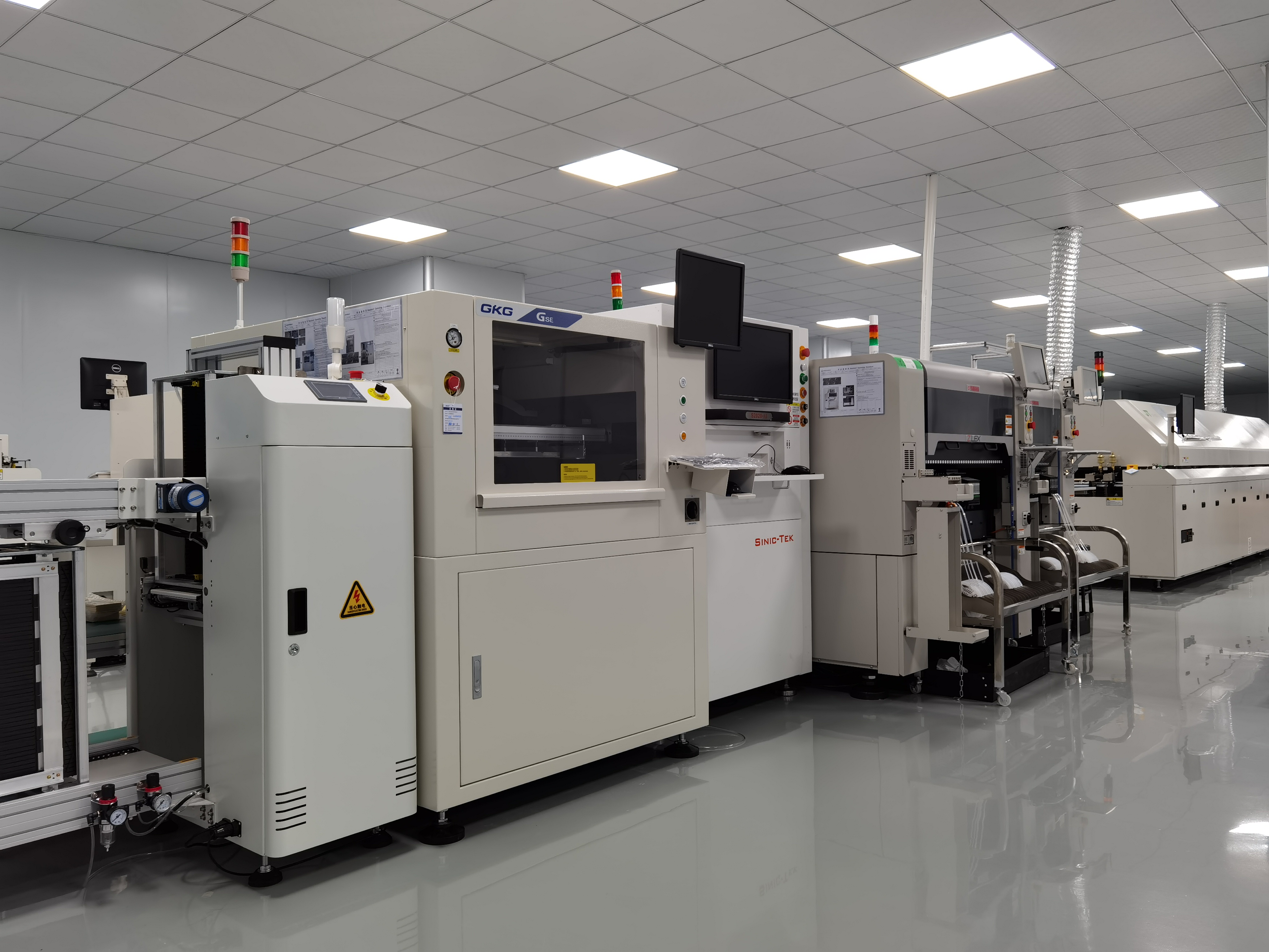
You begin by putting solder paste on the printed circuit board. Solder paste is made of tiny metal powder and flux. The metal melts to make strong, conductive joints. The flux cleans the metal and removes dirt. This step helps parts stick to the board and makes good electrical connections.
There are different ways to put on solder paste. Stencil printing is used for big batches. You put a metal stencil on the board and spread the paste with a squeegee. For small jobs or samples, you can use a syringe or jet dispenser. Each way has its own good points. Stencil printing is fast and even. Syringe dispensing is good for special jobs. Jet dispensing is very exact for tricky boards.
It is very important to put the right amount of solder paste. Too much paste can cause short circuits. Too little paste can make weak joints. LTPCBA uses machines that print solder paste and check it right away. These machines look at the thickness and where the paste is. This lowers mistakes by up to 85%. This step helps your printed circuit boards work well and last longer.
Tip: Always make sure the solder paste is spread evenly. This helps stop problems later in the pcb production and assembly process.
Component Placement
After the solder paste, you place the parts on the board. Pick-and-place machines put the electronic parts on the printed circuit board. These machines are fast and very accurate. LTPCBA uses advanced machines for tiny parts and big connectors. The machines can put up to 46,000 parts every hour.
It is very important to place each part in the right spot. If a part is not placed right, it can cause problems. Even a small mistake can make short circuits or open circuits. LTPCBA’s machines use cameras and sensors to check each part’s spot. Automated Optical Inspection (AOI) checks for errors as small as 0.05 mm. This step makes sure your printed circuit boards work well and last longer.
LTPCBA checks quality all the time. The company often checks its machines and keeps the area clean. This helps stop dust or water from causing problems in your pcb production and assembly.
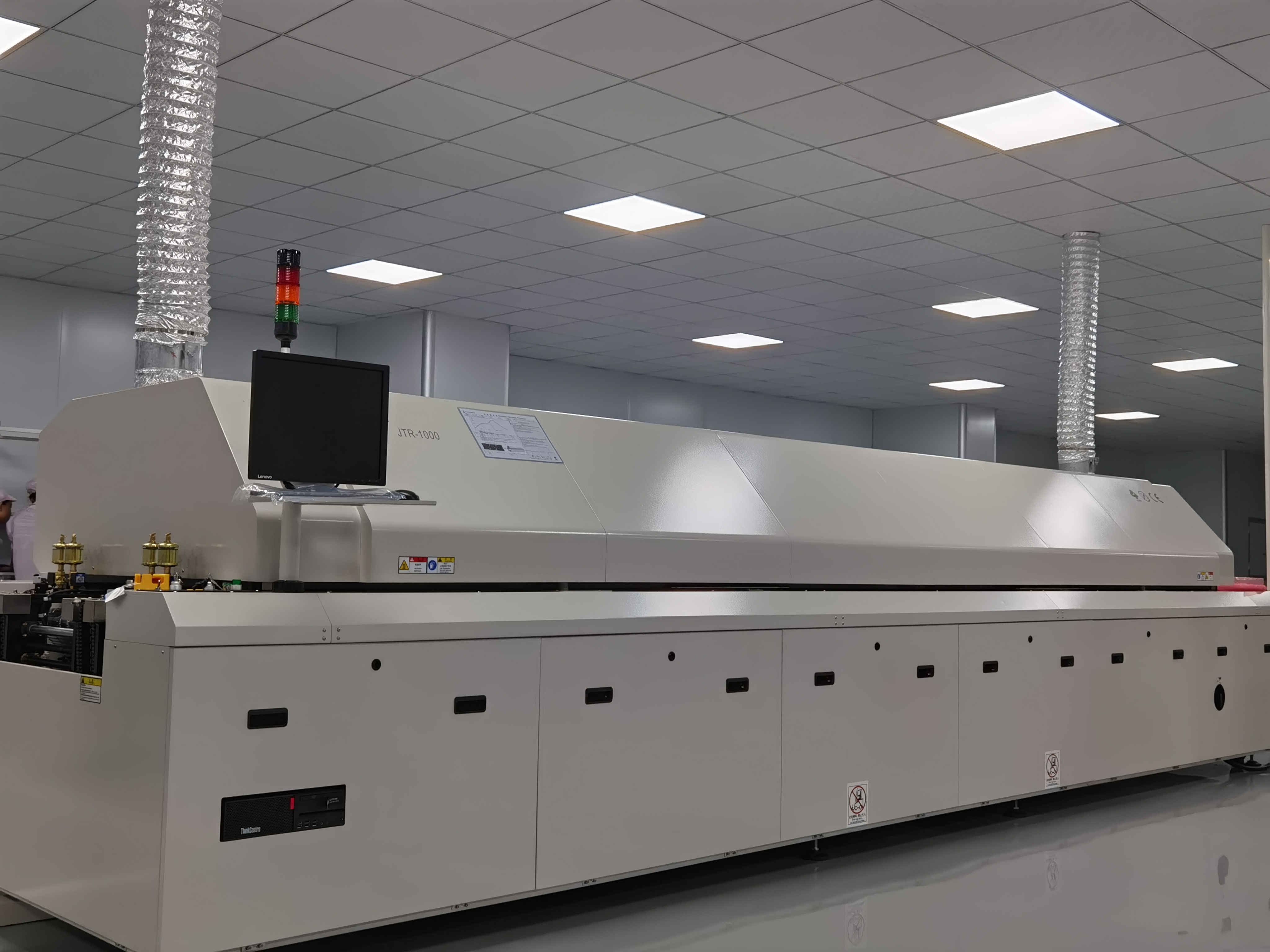
Soldering Methods
After placing the parts, you need to solder them to the printed circuit board. Soldering makes the final electrical and mechanical connections. LTPCBA uses different soldering methods for different boards and parts.
Reflow Soldering: This is used for surface-mount parts. You heat the board in a reflow oven. The solder paste melts and makes strong joints. Reflow soldering gives you good temperature control and works for crowded boards.
Wave Soldering: This is used for through-hole parts. The board goes over a wave of melted solder, which connects all the leads at once. This way is fast and good for making many boards.
Selective Soldering: This is used when you have both surface-mount and through-hole parts. The machine puts solder only where needed, keeping sensitive parts safe.
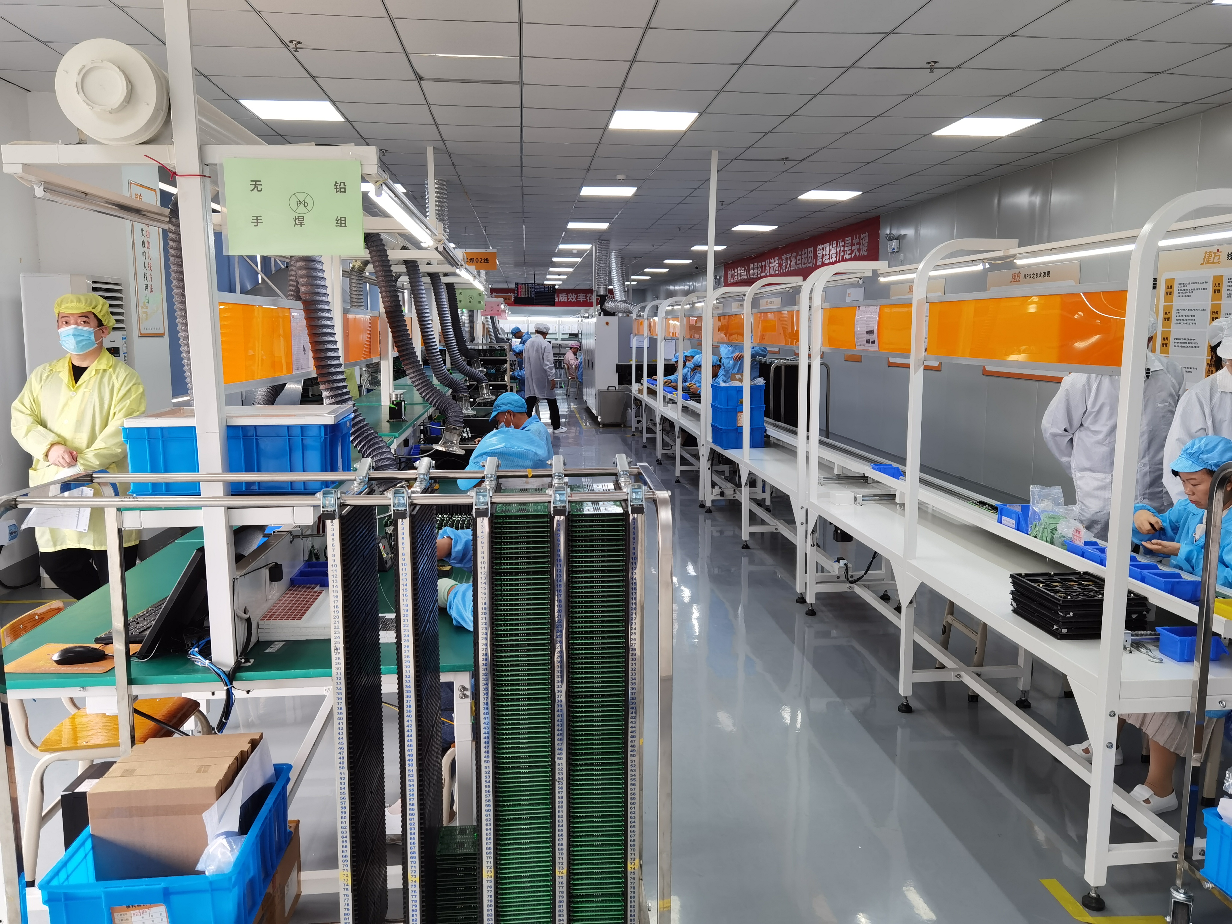
Hand Soldering: This is used for samples, repairs, or special cases. Skilled workers use soldering irons to make or fix connections.
LTPCBA’s machines make sure every solder joint is good. The company uses ovens with exact temperature control and machines to check every joint. This step is very important for your pcb production and assembly to work well.
Soldering Method | Applications | Advantages |
|---|---|---|
Reflow Soldering | Surface-mount components | High precision, supports dense layouts, automated, reliable joints |
Wave Soldering | Through-hole components | Fast, efficient for large batches, strong joints |
Selective Soldering | Mixed assemblies | Solder only where needed, protects sensitive parts |
Hand Soldering | Prototypes, repairs | Flexible, good for small runs or special cases |
Inspection & Testing
You must check and test every printed circuit board after soldering. This step finds problems early and keeps quality high. LTPCBA uses both machines and people to check the boards.
Automated Optical Inspection (AOI): AOI uses cameras to look for missing parts, wrong spots, or bad solder joints. It checks boards fast and finds over 98% of surface problems.
X-ray Inspection: This checks hidden joints, like under BGAs. X-rays can see inside the board and find problems you cannot see.
Functional Testing: You test the finished board to make sure it works right. The test acts like real use.
In-Circuit Testing (ICT): This checks each part’s electrical connections. It finds problems fast and well.
Flying Probe Testing: This is used for samples or small batches. Probes move over the board and test each spot.
LTPCBA’s machines and AOI help find more problems and lower rework. The company uses real-time data to change the process and keep quality high. You get printed circuit boards you can trust.
Final Steps & Packaging
After checking, you finish the pcb production and assembly process by cleaning and packing. You wash and dry the printed circuit board to remove leftover flux or dirt. LTPCBA can add a special coating if you need more protection.
You pack the boards in anti-static bags and moisture barriers. LTPCBA follows IPC 1601 rules and uses vacuum bags, drying packs, and humidity cards. This keeps your boards safe from static and water during shipping. The company adds barcodes and labels for tracking. You can ask for special packing or extra papers, like certificates.
Before shipping, LTPCBA checks what is in the package and gets all shipping papers ready. The company uses trusted shippers like DHL, FedEx, or UPS. You get an email when your order ships. If you have extra parts, LTPCBA sends them back if you want.
Note: LTPCBA answers fast, so you get quotes in 2-3 days and help any time. You can fix problems quickly and keep your project moving.
Every step in making and putting together a pcb is important.
Careful checking and testing help stop problems like layers not matching or bad soldering.
LTPCBA uses smart machines and good controls to make sure you get boards you can trust.
Expert help means your boards are made faster, with fewer mistakes, and you get good support for your next pcb job.
FAQ
What files do you need to start PCB production and assembly?
You need Gerber files, a Bill of Materials (BOM), and pick-and-place files. These files help your manufacturer build your board correctly.
How long does the PCB assembly process take with LTPCBA?
You usually get a quote in 2-3 days. Production and assembly often finish within 7-10 working days, depending on your order size.
Can you order both prototypes and large batches from LTPCBA?
Yes! LTPCBA handles small prototypes and larger production runs. You get the same quality and support for any order size.
See Also
Comprehensive Overview of PCBA Manufacturing for All Skill Levels
PCBA Services Explained: From Production Through Final Testing
Understanding Complete Turnkey PCB Assembly And Manufacturing Process
Essential Materials Required For Successful PCBA Manufacturing
Quality Assurance In Modern Turnkey PCBA Manufacturing Facilities