Key Steps for Optimizing Your HDI PCB Assembly
You can optimize hdi pcb assembly by following a methodical approach in both design and manufacturing. Reliable hdi pcb assembly performance depends on careful material selection, precise stackup, and advanced via management. Many hdi pcb assembly boards face reliability issues such as microvia fractures or insulation resistance degradation.
Issue | Description | Solutions |
|---|---|---|
Microvia fractures | Occur during temperature cycling due to insufficient via wall copper thickness, CTE mismatch, and drilling residues. | Optimize pulse plating, use CTE-matched dielectrics, implement plasma cleaning. |
Insulation resistance degradation | Results from moisture absorption or interface delamination during damp heat testing. | Use low-moisture-absorption dielectrics, enhance resin-copper adhesion, apply moisture-resistant coatings. |
To achieve consistent results with hdi pcb assembly, it’s essential to use best practices that address these challenges and ensure long-term reliability.
Key Takeaways
Optimize material selection and stackup to enhance signal integrity and thermal management in HDI PCB designs.
Address common reliability issues like microvia fractures by using CTE-matched materials and implementing proper cleaning techniques.
Follow design for manufacturability (DFM) guidelines to reduce defects and improve the ease of production for HDI PCBs.
HDI PCB Assembly Overview
What Is HDI
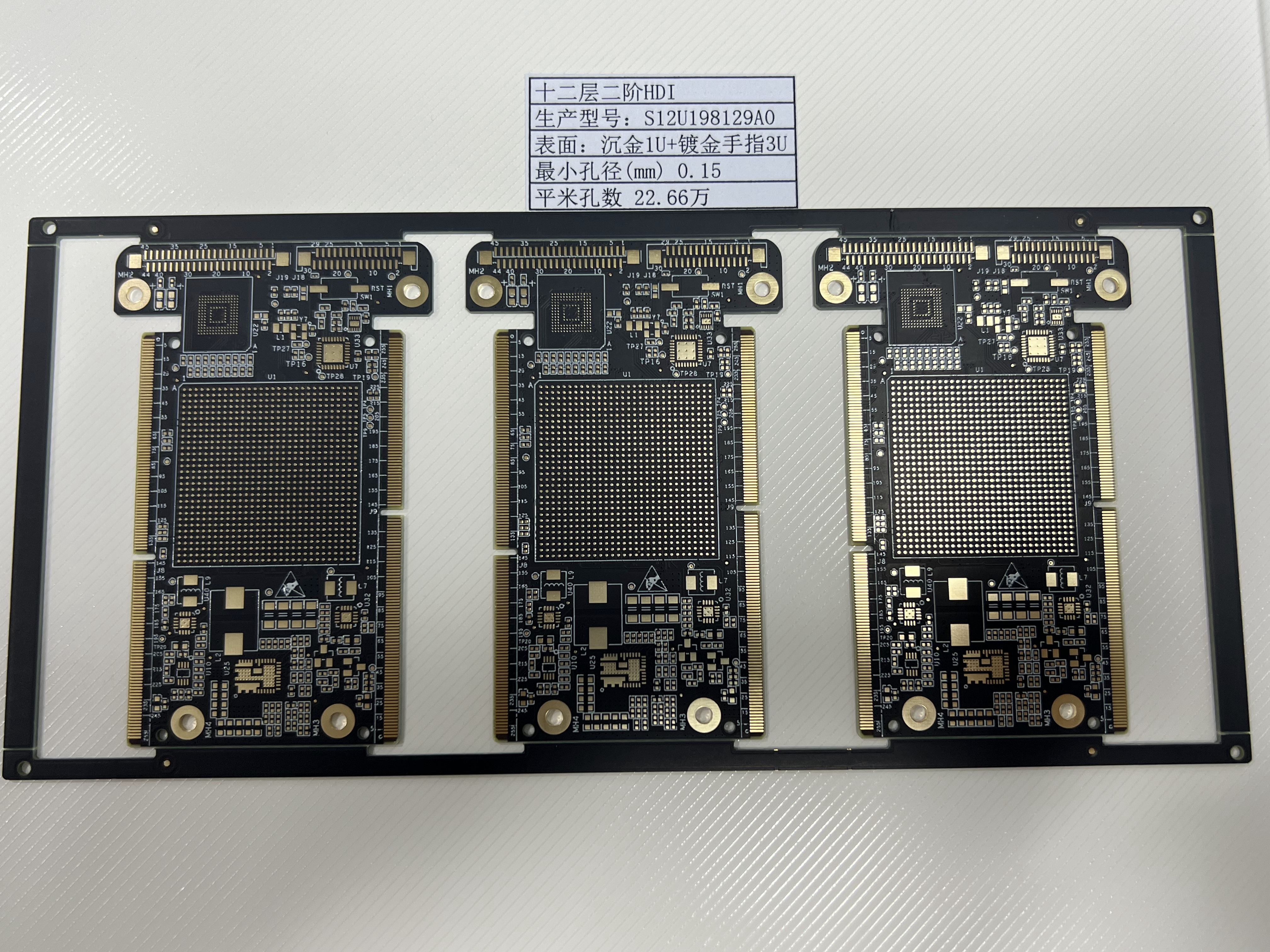
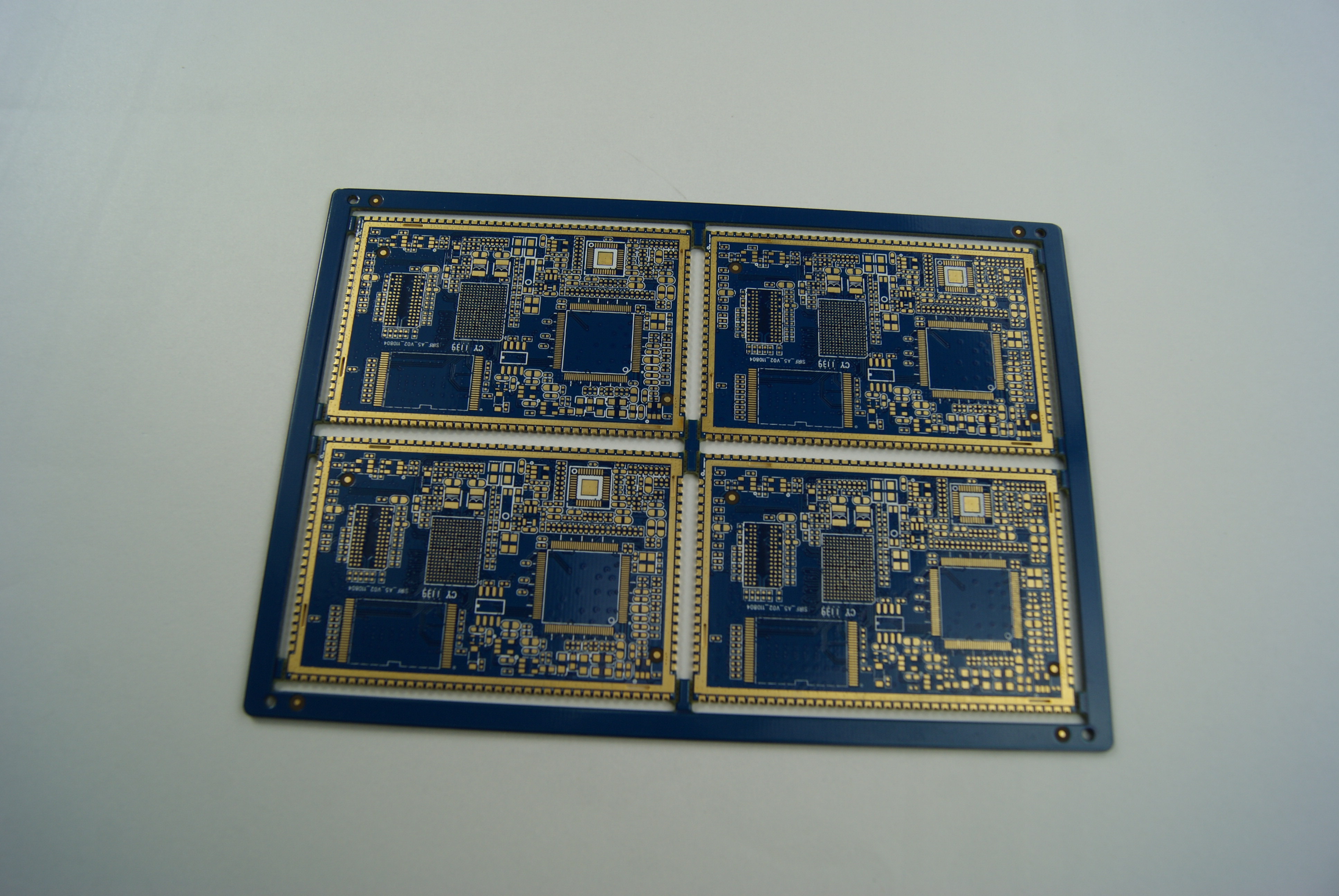
You encounter HDI technology in many modern electronics. HDI stands for high-density interconnect, which describes printed circuit boards with a higher wiring density than traditional designs. HDI PCBs use microvias, blind vias, and buried vias to connect layers. These features allow you to fit more components and connections into a smaller space.
Industry standards classify HDI PCBs by via type and size.
Type | Description | Size |
|---|---|---|
Type I | 0.15 mm (6 mils) or less | |
Type II | Blind via features | 0.15 mm to 0.50 mm (6-20 mils) |
Type III | Through-hole via features | Greater than 0.50 mm (20 mils) |
HDI PCBs use thinner traces and smaller drill-to-copper ratios. You benefit from increased reliability and higher functionality because these boards support advanced layering techniques.
Why HDI PCB Assembly Matters
You rely on HDI PCB assembly for devices that demand speed, miniaturization, and reliability. High-density interconnect boards appear in wearable technology, medical equipment, aerospace, and automotive electronics.
Application | Description |
|---|---|
Wearable technology | Miniaturization and low power consumption |
Medical equipment | High-precision imaging and diagnosis |
Aerospace and defense | High-frequency and high-reliability operation |
Automotive electronics | High-performance computing and control |
HDI PCB assembly improves electrical performance. You see reduced delays and enhanced signal integrity because shorter signal paths and fewer channels minimize noise and electromagnetic interference. High-density interconnect designs support data rates above 1 Gbps, which is essential for 5G and Wi-Fi 6 devices. You also gain reliability benefits, such as stacked vias that withstand extreme conditions and via-in-pad technology that shortens signal paths.
Tip: When you plan your HDI PCB assembly, collaborate early with your design and manufacturing teams. Use advanced tools that follow IPC standards and conduct thorough testing to ensure quality.
HDI PCB Design Essentials
Material and Stackup
You start every successful hdi pcb design by choosing the right materials and stackup. The materials you select affect signal integrity, thermal management, and overall reliability. You need to understand the dielectric properties of each material to control impedance and minimize signal loss.
Material | Dielectric Constant (Dk) | Dissipation Factor (Df) | Key Features |
|---|---|---|---|
Isola FR408HR | Higher Dk | Higher Df | Good for general hdi applications |
Nelco N4000-13 SI | Low Dk | Steady electrical properties | Reliable for signal integrity |
Panasonic Megtron 6 | Very low Df | Easy for laser-drilled holes | Ideal for complex hdi stackups |
PTFE | Low Dk | Low Df | Excellent for high-frequency signal |
Ceramic-filled epoxy | Low Dk | Low Df | Stable for advanced hdi designs |
Tip: You achieve optimal signal integrity in high-frequency hdi pcb design by using materials with a dielectric constant between 2.1 and 3.5.
You must also consider how the stackup arrangement impacts heat dissipation and board reliability. Effective thermal management prevents board failure and performance issues. You control heat by selecting materials with good thermal properties and arranging layers to spread heat evenly. LTPCBA uses advanced technology to build multilayer stackups that support complex hdi requirements. You benefit from their quality assurance and expertise in handling challenging printed circuit boards.
Signal Integrity
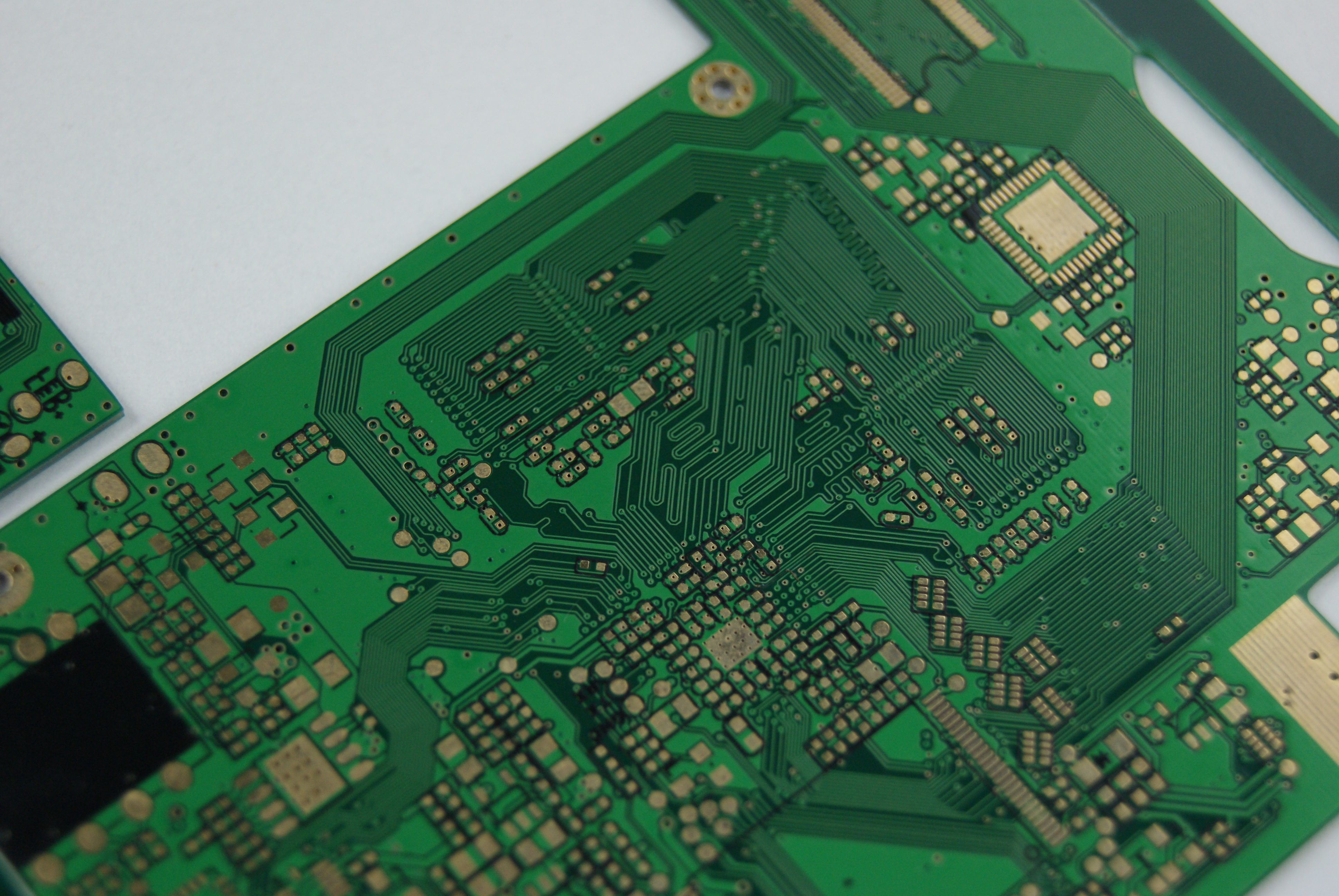
You face unique signal integrity challenges in hdi pcb design because of close trace packing and high frequencies. You must address issues like crosstalk, reflections, and timing mismatches. You improve signal integrity by using controlled impedance routing, matching trace widths and spacing, and keeping differential pairs close and equal in length.
Challenge | Solution |
|---|---|
Signal integrity issues due to close trace packing and high frequencies | Use controlled impedance routing to match trace widths and spacing to prevent reflections. |
Crosstalk and reflection problems | Route differential pairs properly, keeping them close and of equal length. |
Timing issues with signal arrival | Match trace lengths for signals that need to arrive simultaneously, like clocks or data buses. |
Interference with sensitive signals | Add guard traces by placing grounded traces next to sensitive signals. |
You use simulation tools to analyze signal integrity before and after layout. Pre-layout simulations help you predict signal behavior, while post-layout simulations let you check geometry-dependent issues. You compare simulation results with real measurements to ensure accuracy. You need built-in simulation capabilities to analyze timing and EMI during the design phase. LTPCBA supports you with advanced design software and quality assurance processes, helping you maintain signal integrity in every hdi pcb design.
Note: You target impedance values between 50 and 100 ohms for high-speed signals in hdi printed circuit boards.
Via Management
You rely on vias to connect layers in hdi pcb design. You choose from several via types, each with specific benefits and challenges. IPC standards guide you in selecting the right via type and size for your application.
Type | Description |
|---|---|
Allows only a single micro via layer on either side of the pcb. | |
Type 2 | Allows micro vias as in Type 1, plus through hole vias connection within the outer layers. |
Type 3 | Provides two additional hdi layers beyond Type 2. |
Type 4 | Represents a passive substrate with no electrical functions. |
Type 5 | A coreless construction using hdi layers. |
Type 6 | An ELIC type of construction using layer pairs. |
Via Sizes and Specifications | Details |
|---|---|
Line Spaces | 100 micrometers |
Via Diameters | Less than 150 micrometers |
Capture Pads | Less than 400 micrometers |
Connection Pad Density | More than 20 pads per square centimeter |
You use via-in-pad technology to shorten signal paths and improve signal integrity. You also save space and enhance thermal management by routing signals directly on component pads. You must work with manufacturers like LTPCBA who have the equipment and expertise to handle complex via structures in hdi pcb design.
Tip: You improve reliability and manufacturability by optimizing via placement and using plasma cleaning to remove drilling residues.
Component Placement
You achieve high performance in hdi pcb design by placing components accurately. You avoid short circuits and connectivity issues by using automated pick-and-place machines calibrated to tight tolerances. You implement controlled impedance routing by managing trace width, spacing, and dielectric thickness. You use differential pair routing to reduce noise and enhance signal stability. You optimize ground and power planes to shield signals and minimize crosstalk.
You maintain controlled impedance for high-speed signals, targeting 50 ohms.
You space high-speed traces apart or use ground planes to reduce crosstalk.
You keep trace lengths short to minimize signal delay.
LTPCBA uses advanced assembly technology and quality assurance to ensure precise component placement in every hdi pcb design. You benefit from their expertise in assembling complex printed circuit boards with high pass rates.
Note: You improve signal integrity and reduce signal loss by following best practices in component placement and routing.
Manufacturing for HDI PCB Assembly
Lamination
You start the manufacturing process for hdi pcb assembly with lamination. This step builds the foundation for your board’s structure and reliability. You create individual layer pairs, image and etch them, then bond them together using prepreg sheets. Unlike standard pcb manufacturing, you laminate layers one pair at a time. This sequential lamination helps you control layer registration and maintain the alignment needed for high-speed signals and microvias.
Here is how the lamination process works for hdi pcb assembly:
You fabricate and etch each layer pair.
You laminate the pairs together, one cycle at a time.
After each cycle, you drill and fill vias to connect the layers.
You repeat the process, sometimes up to five cycles, depending on the complexity of your pcb.
You maintain controlled impedance traces to support high-speed signals and signal integrity.
You may need two to four lamination cycles for most hdi pcb designs. The number of cycles depends on the type of microvias, the starting and ending points of blind and buried vias, and whether you use foil or core construction. You must watch for defects like delamination, voids, warpage, and registration issues. You can detect these problems with visual inspection, flatness gauges, X-ray imaging, or acoustic microscopy.
LTPCBA uses automated lamination systems and advanced inspection tools to ensure every hdi pcb meets strict international standards like ISO, IATF, and UL. You benefit from their expertise and quality assurance, which help you avoid common lamination defects and achieve reliable results.
Drilling and Microvias
You rely on precise drilling to create microvias and connect the layers in your hdi pcb. Laser drilling is the main technology for microvias because it offers tight tolerances, often as precise as ±10 microns. You use thin dielectric layers, usually less than 0.1 mm, to keep the aspect ratio of micro vias around 0.8:1. Lower aspect ratios help you achieve better copper plating and stronger via connections.
You need to manage a large number of microvias and vias in hdi pcb assembly. You must ensure that each micro via is clean and free of debris to support high-speed signals. LTPCBA uses automated drilling equipment to handle complex via patterns and maintain the accuracy needed for advanced pcb designs. Their quick response and support for both prototypes and mid-volume production help you move from design to finished board without delays.
Tip: You improve the reliability of your hdi pcb by optimizing the placement and size of microvias and vias, especially when routing high-speed signals.
Metalization
You must metallize the walls of your microvias and vias to create strong electrical connections between layers. The metallization process is critical for hdi pcb reliability, especially when you use many micro vias for high-speed signals. Two main processes are used: electroless copper and direct metallization.
Metallization Process | Advantages | Disadvantages |
|---|---|---|
Electroless Copper | Widely used, effective in low-density designs. | Reliability issues in high-density designs. |
Direct Metallization | Eliminates hydrogen gas production, improves uniformity and strength. | Newer method, may require more advanced equipment. |
Electroless copper is common, but you may see reliability problems in high-density hdi pcb designs with many microvias. Direct metallization is becoming more popular because it avoids issues like hydrogen gas formation and provides better uniformity and strength for micro vias. LTPCBA uses advanced metallization techniques to ensure every via and microvia supports high-speed signals and long-term reliability.
Surface Finish
You choose the right surface finish to improve solderability and protect your hdi pcb from environmental damage. The surface finish affects how well solder wets and bonds to copper, which is important for strong joints and reliable high-speed signals. Finishes like ENIG (Electroless Nickel Immersion Gold) and Immersion Silver resist oxidation and promote excellent solder wetting. OSP (Organic Solderability Preservative) adds a protective layer that enhances solderability.
Different surface finishes also influence the formation of intermetallic bonds, which are essential for both mechanical and electrical connections. Your choice of finish impacts the pcb’s resistance to moisture, heat, and other environmental factors. LTPCBA offers a range of surface finishes to match your hdi pcb requirements, ensuring your microvias and vias remain reliable for the life of your product.
Note: You improve the long-term reliability of your hdi pcb by selecting a surface finish that matches your application and supports high-speed signals.
You can trust LTPCBA’s automated systems and strict quality controls to deliver hdi pcb assemblies that meet international standards. Their quick response and support for prototype to mid-volume production help you bring your designs to market faster and with greater confidence.
Overcoming HDI Challenges
Warpage and Reliability
You often face warpage issues in hdi pcb assemblies, especially when you use higher wiring density and multiple vias. Warpage can affect performance and cause failures in common applications of hdi pcbs. You can reduce warpage by following these best design practices:
Optimize layer stacking and add support structures.
Control lamination parameters and use proper cooling.
Maintain temperature and humidity during assembly.
Inspect for warpage and use stress-relief techniques after assembly.
You also need to ensure long-term performance. You can use in-circuit testing to check electrical connectivity and functional testing to validate performance under real-world conditions. These steps help you maintain effective signal routing and reliable performance in your hdi pcb.
Manufacturability
You improve manufacturability by planning your hdi pcb design with production in mind. HDI pcbs require precision because you work with multiple layers, tight trace spacing, and many vias. To make manufacturing easier and boost performance, you should:
Optimize layer stack-ups with symmetrical builds to reduce warpage.
Limit buried vias and plan via placement to save processing time.
Select materials that meet electrical needs and are cost-effective.
Use symmetrical stacks and alternate signal and ground planes for controlled impedance. Place high-speed signals close to reference planes for better performance.
You also benefit from using via-in-pad technology and effective signal routing strategies. These methods help you achieve shorter signal paths and higher wiring density, which are key for performance in common applications of hdi pcbs.
EMI and Shielding
You must control electromagnetic interference (EMI) to protect signal integrity and maintain performance. You can use several shielding techniques in your hdi pcb:
Apply silver shields or silver ink layers for circuits without impedance control.
Use shield films to provide high EMI shielding and protect against moisture.
Add ground planes and use effective signal routing strategies to reduce EMI.
Shield films also improve the rigidity and reliability of flexible hdi pcbs. By combining these methods with careful routing and via management, you ensure your hdi pcb delivers strong performance and meets the demands of higher wiring density.
Best Practices and Tips
DFM Guidelines
You improve your hdi pcb assembly by following strong design for manufacturability (DFM) guidelines. These rules help you reduce defects and make your design easier to build. Use the table below to check the most important DFM points:
Guideline | Description |
|---|---|
Clearance between vias | Keep at least 0.15” to 0.2” between exposed vias and other conductors. Use tented or plugged vias in BGA designs. |
Minimum trace width and spacing | Match your design to the manufacturer’s limits for reliable pcb production. |
Component orientation | Place components to simplify routing and reduce signal interference. |
Copper balance | Distribute copper evenly to avoid plating or etching problems. |
Solder mask design | Define solderable areas clearly to prevent solder bridging. |
Tooling holes and fiducials | Add these for accurate assembly alignment. |
You also need to set the right hole size and pad diameter for good solder joints. LTPCBA’s technical support team can review your design and help you meet these DFM standards. Their automated optical inspection (AOI) ensures high quality at every step.
Prototyping
You validate your hdi pcb design by building and testing prototypes before mass production. Start with EVT samples to check your design. Make 5–25 sample boards using the same process as full production. Test each board for function, electrical performance, and environmental durability. If you find issues, update your design and repeat testing. Once your design passes all tests, you can move to full production with confidence. LTPCBA supports you with fast prototyping and a high pass rate, so you can trust your results.
Documentation
You keep your hdi pcb project on track with clear documentation. Include compliance and certification status, defect classification, and testing protocols. Use standards like IPC-A-610, ISO 9001, RoHS, and UL to ensure quality and traceability. Good documentation helps you communicate your design needs and supports quality control. LTPCBA’s customer-focused service helps you organize your files and meet all documentation requirements for your pcb assembly.
You optimize hdi pcb assembly by following a clear checklist.
Align footprints with datasheets
Mark pin 1 and polarity
Specify accurate BOM details
Group components by function
Maintain proper clearances
Prevent silkscreen overlap
Add panel gaps
Apply these steps for reliable hdi pcb assembly. LTPCBA supports your hdi pcb assembly needs.
FAQ
What is the main advantage of HDI PCB assembly?
You achieve higher wiring density and better signal integrity. HDI PCBs allow you to build smaller, faster, and more reliable electronic devices.
How do you prevent microvia failures in HDI PCBs?
You select CTE-matched materials, optimize copper plating, and use plasma cleaning. These steps help you avoid microvia fractures and improve reliability.
Why should you choose LTPCBA for HDI PCB assembly?
Benefit | Description |
|---|---|
You get strict ISO, IATF, UL compliance. | |
Fast Support | You receive quick quotes and 24-hour help. |
High Pass Rate | You benefit from a 99.5% delivery success. |
See Also
Enhancing SMT PCB Assembly for Optimal Efficiency and Output
Essential Guidelines for Safe HDI PCB Surface Mount Assembly
Crucial Actions to Boost PCBA Reliability Over Time