The History and Evolution of Multilayer PCBA Technology
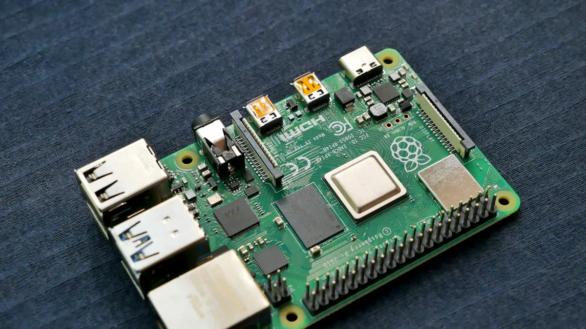
Multilayer pcba technology utilizes two or more inner layers to build compact and powerful electronic circuits. Multilayer pcba is essential in high-performance computing, consumer electronics, and defense systems due to its lightweight and durable design.
Year | Market Size (USD Billion) | CAGR (%) |
|---|---|---|
2022 | N/A | |
2023 | 28.66 | N/A |
2032 | 38.57 | 3.36 |
Understanding the history of multilayer pcba advancements helps explain their increasing impact on daily life and various industries.
Key Takeaways
Multilayer PCBA technology allows for compact and powerful electronic circuits, essential for high-performance devices.
The evolution of multilayer PCBs has led to increased circuit density, improved reliability, and miniaturization of electronic devices.
Modern multilayer PCBs support various industries, including consumer electronics and medical devices, by enhancing functionality and durability.
Origins of Multilayer PCBs
Early Concepts
The history of pcbs began with inventive ideas that shaped the future of electronics.
Albert Hanson patented a flat foil conductor on an insulating board in 1903. His design featured through-hole construction and conductors on both sides, laying the groundwork for modern printed circuit board technology.
Charles Ducas introduced 'printed wiring' in 1925. He used conductive inks to create electrical pathways on insulated surfaces, which marked a significant step in pcb development.
Paul Eisler developed the first modern pcb concept in the 1930s. He etched circuits onto copper foil laminated onto a non-conductive substrate, which became a standard for future pcb manufacturing.
Industries such as radio, television, and early computing experimented with multilayer pcb concepts during the 1950s and 1960s. The introduction of Plated Through-Hole (PTH) technology enabled the creation of double-sided and multi-layered boards, which improved circuit density and reliability.
Early inventors and engineers faced many challenges. Complex manufacturing processes required precision and advanced machinery. Higher design costs made small production runs expensive. Thermal management issues and signal interference posed risks to performance. Diagnosing faults became more difficult as layers increased, leading to higher maintenance costs.
Challenge | Description | Impact |
|---|---|---|
Involves intricate steps requiring precision and advanced machinery. | Increases risk of defects and misalignments, necessitating strict quality assurance. | |
Higher Design Costs | Requires specialized software and skilled engineers for design. | Small production runs can be prohibitively expensive for businesses with limited budgets. |
Thermal Management Issues | Higher layer density leads to heat generation that must be managed. | Improper heat dissipation can cause electronic failures and reduced performance. |
Signal Interference and Crosstalk | Closely packed layers increase risk of EMI and crosstalk. | Can lead to malfunctions in critical applications if not properly managed. |
Repair and Maintenance Complexity | Diagnosing faults is more challenging due to multiple layers. | Higher maintenance costs and potential downtime for repairs. |
1960s Breakthroughs
The 1960s marked a turning point in the history of pcbs. The advent of integrated circuits (ICs) transformed pcb technology. ICs replaced multiple discrete components with a single chip, which allowed engineers to increase conductor layers within pcbs. This development led to the practical manufacturing of multi-layer pcbs.
Multi-layered boards enabled intricate and compact electronic designs. Stacking multiple layers of conductive and insulating materials improved signal integrity and reduced electromagnetic interference. These advancements allowed for the miniaturization of electronic devices.
Year | Advancement/Impact |
|---|---|
1960s | Introduction of double-sided pcbs, improving circuit density. |
1970s | Development of multi-layer pcbs with 4+ layers for advanced applications. |
1980s | Miniaturization of electronic components, driving demand for smaller pcbs. |
Impact | Enabled smaller, more powerful computers and expanded consumer electronics. |
Several companies and research institutions played key roles in commercializing multilayer pcb technology.
Year | Company/Institution | Contribution |
|---|---|---|
1962 | Japan Printed Circuit Industry Association | Established to promote pcb industry in Japan |
1964 | American Optical Circuit Company | Developed thick copper electroless copper plating solution (CC-4 solution) |
1964 | Hitachi Chemical Company | Introduced CC-4 technology for GE substrate of pcb |
1965 | Various material manufacturers in Japan | Began mass production of GE substrates |
1968 | Development of medium and large-scale integrated circuits | Led to the production of hole metallized double-sided pcbs and flexible pcbs |
1970s-1980s Advancements
During the 1970s and 1980s, multi-layered boards became smaller and more efficient. Hot-air soldering methods improved soldering efficiency and repair processes. The introduction of microprocessors opened new opportunities for electronic devices. Consumer electronics demand surged, which required smaller and more functional pcbs.
Surface mount assembly emerged in the 1980s, reducing production costs while maintaining functionality. Electronic design automation (EDA) software revolutionized pcb design and manufacturing. The development of liquid photo imageable masks became standard, indicating a shift toward sophisticated manufacturing processes.
In this period, multi-layer pcbs evolved from basic single-layer designs to complex structures. Typical layer counts reached 2, 4, 6, and eventually up to 20 layers. The need for higher density and complexity in circuits drove this evolution.
Year | Advancement/Impact |
|---|---|
1970s | PCBs became smaller, and hot-air soldering methods improved soldering efficiency and repair processes. |
1980s | Surface mount assembly and EDA software revolutionized pcb design and manufacturing. |
Impact | Expansion of consumer electronics and miniaturization of devices. |
Industry standards evolved to accommodate these changes. The emergence of surface-mount technology and the expansion of multilayer pcb adoption were significant. The introduction of photo-imageable solder masks became common, which influenced regulatory and industry standards.
The 1970s and 1980s marked a period of rapid growth for the printed circuit board industry. Engineers and manufacturers responded to new challenges with innovative solutions, setting the stage for modern multilayer pcb technology.
Evolution of Multi-layered Circuit Boards
Packing Density and Performance
Engineers in the 1980s faced new challenges as electronic devices became smaller and more powerful. The demand for higher packing density in multilayer pcba increased rapidly. Several factors drove this trend:
Factor | Explanation |
|---|---|
Higher density in IC packaging necessitated more interconnections, leading to multilayer designs. | |
Need for more interconnections | Complex electronic circuits required more connections than single or double-layer boards could provide. |
Challenges in circuit board design | Issues like noise, stray capacitance, and crosstalk made multilayer boards essential for performance. |
Designers responded by stacking more layers in multilayer pcbs. This approach allowed them to fit more components and connections into a smaller space. As a result, electronic devices gained new capabilities and improved reliability.
Higher integration of functions in electronic devices became possible.
Reduction in component count led to simpler designs.
Enhanced thermal management capabilities improved device safety.
Advanced packaging technologies like SoC, SiP, and SoP contributed to miniaturization and operational efficiency.
The evolution of pcb design during this period set the stage for high advancement in pcbs. Multi-layered circuit boards became the foundation for modern electronics.
Microvia and HDI Technology
In the 1990s, manufacturers introduced microvia technology to address the limitations of traditional multilayer pcbs. Microvias are tiny holes that connect layers within a printed circuit board. This innovation enabled compact designs and higher functionality.
Microvia technology allows intricate circuitry and improved performance in electronic devices.
Engineers use microvias to create advanced multilayer pcbs with precise connections.
The development of high-density interconnect technology transformed multilayer pcba capabilities. The timeline below highlights key milestones:
Year | Development | |
|---|---|---|
1980 | Research on reducing via size | |
1984 | First production build-up boards | Enabled more compact designs |
1991 | Introduction of IBM’s SLC technology | Paved the way for mass production of HDI boards |
1990s | Growth in consumer electronics | Increased demand for denser interconnections and smaller form factors |
Engineers adopted microvia and high-density interconnect solutions to meet the demand for miniaturization, increased component density, improved signal integrity, and enhanced thermal management. These advances made multilayer pcba suitable for smartphones, tablets, and other compact devices.
However, these technologies also increased production costs and complexity. HDI pcbs can cost two to five times more than standard multilayer boards. Design complexity rises by 15% to 25% due to tighter spacing and precise via placement. Specialized equipment and laser drilling add to manufacturing expenses. Stacked microvias require precise alignment and copper filling, which further increases costs. Staggered microvias simplify manufacturing and help reduce costs for multilayer pcbs.
Modern Multilayer PCBA
Today, multilayer pcba technology supports a wide range of industries. Modern multilayer pcbs offer enhanced functionality, improved durability, and superior performance. The table below compares key features and specifications of modern multilayer pcbs with earlier generations:
Feature/Specification | Modern Multilayer PCBs | Earlier Generations |
|---|---|---|
Reliability | Strong bonding for better resistance | Lower resistance to environmental factors |
Assembly and Testing | Simplified due to integration | More complex with multiple boards |
Cost | Lower overall costs due to single board usage | Higher costs with multiple boards |
Design Flexibility | Easier last-minute modifications | Limited flexibility |
Manufacturing Processes | Advanced techniques like LDI and semi-additive plating | Older methods with lower precision |
Thermal Management | Enhanced heat dissipation with dedicated layers | Less effective thermal management |
EMI Shielding | Superior due to close proximity of planes | Weaker shielding |
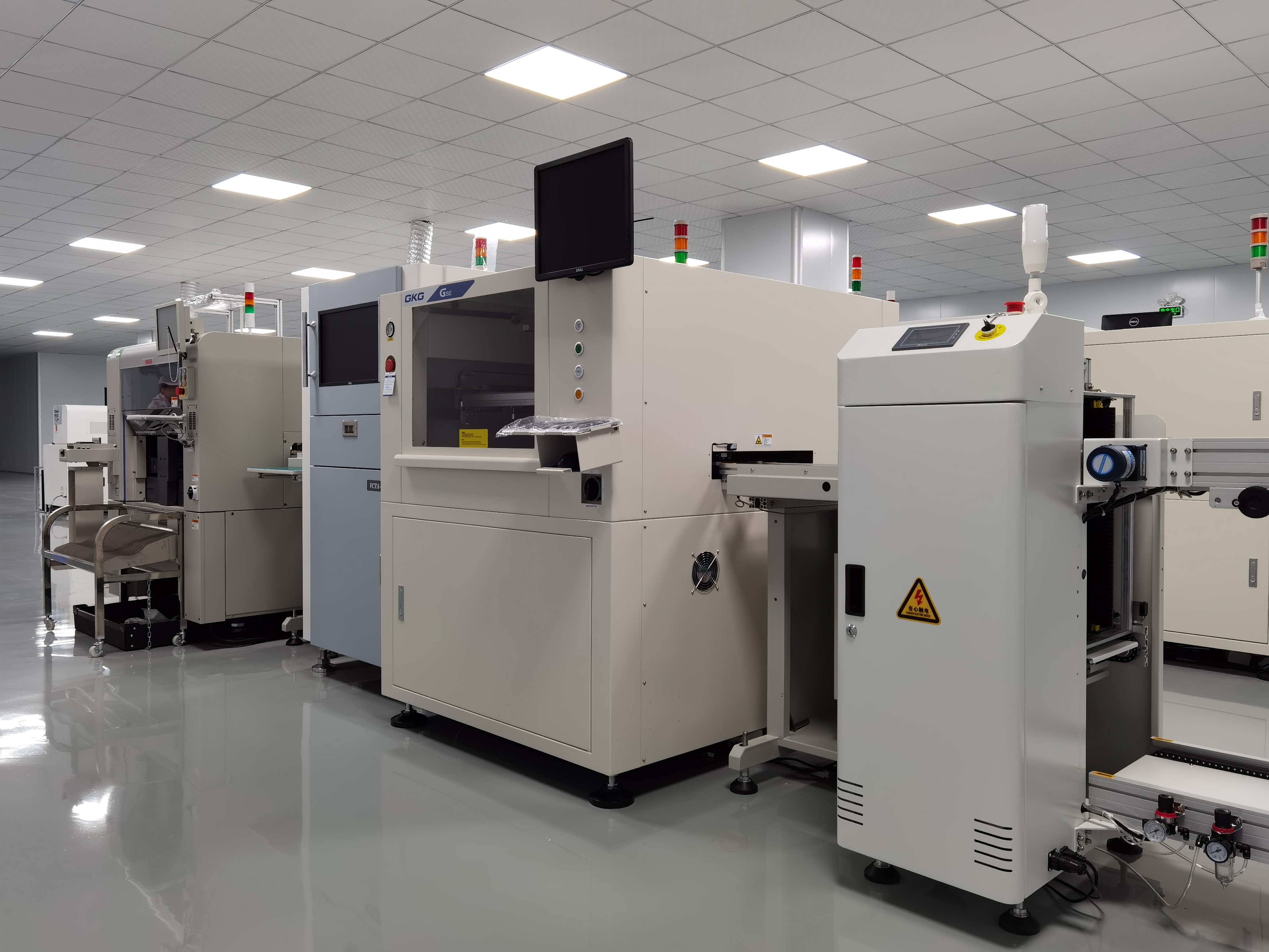
Modern multilayer pcba provides enhanced functionality in a compact size, improved durability and reliability, and better EMI shielding. Automated systems and advanced inspection techniques like Automated Optical Inspection (AOI) and X-ray inspection ensure higher reliability. Precision in component placement through automated machines has become standard.
Industries that rely most heavily on advanced multilayer pcba include consumer electronics, telecommunications, automotive, medical devices, and aerospace and defense.
Industry | Common Applications |
|---|---|
Consumer Electronics | Smartphones, Tablets, Wearable Devices, Home Appliances |
Telecommunications | Routers, Switches, Base Stations, Satellite Communication |
Automotive | Infotainment Systems, Advanced Driver Assistance Systems (ADAS), Electric and Hybrid Vehicles |
Medical Devices | Diagnostic Equipment, Implantable Devices, Portable Medical Devices |
Aerospace and Defense | Durable electronics for extreme conditions, including various applications in aerospace and defense sectors |
Multilayer pcba plays a crucial role in advanced medical devices and aerospace systems. MRI machines, pacemakers, and diagnostic equipment require high-precision pcbs for reliable operation. Radar systems and avionics benefit from the high reliability and performance of multilayer pcbs. Controlled impedance and fast communication enable precise movements in surgical robots and high-speed data processing in imaging equipment.
Manufacturers use advanced design software to create and validate complex multilayer boards before production. This approach accelerates the evolution of pcb technology and supports ongoing innovation.
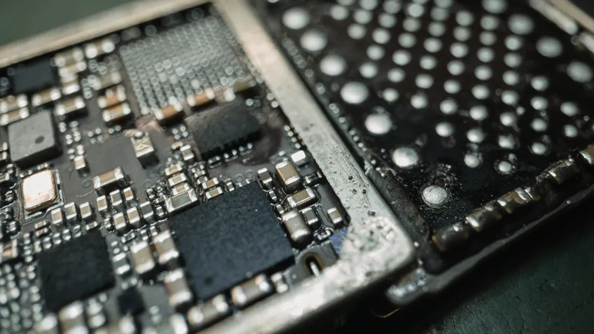
Common failure modes in modern multilayer pcba include layer misalignment, poor via plating, delamination, trace width inconsistencies, burnt components, environmental factors, and soldering issues. Automated quality control processes and strict manufacturing tolerances help mitigate these risks.
Modern multilayer pcba technology continues to evolve, driving progress in electronics and enabling new applications across industries.
Key milestones in multilayer PCBA include the introduction of multilayer boards, plated through-hole technology, and surface mount assembly. These advances enabled smaller, more powerful devices. Today, engineers use advanced materials and automation. The market continues to grow as miniaturization, sustainability, and new applications like 5G and IoT drive innovation.
FAQ
What is the main advantage of using multi-layer pcbs in modern technology?
Multi-layer pcbs allow engineers to fit more circuits into smaller spaces. This technology supports faster, more reliable devices in many industries.
How does a printed circuit board differ from older wiring methods?
A printed circuit board uses flat layers to connect components. Older methods used wires, which made devices larger and less reliable.
Why do industries choose advanced pcb technology for critical applications?
Industries select advanced pcb technology because it improves performance, increases reliability, and supports complex designs. Printed circuit board solutions help meet strict safety and quality standards.
See Also
Understanding PCBA: Key Components and Their Functions
DIP PCBA Production: Processes, Quality Assurance, and Uses
Comprehensive Overview of PCBA Manufacturing Techniques
Combining SMT and DIP Techniques for Enhanced PCB Performance