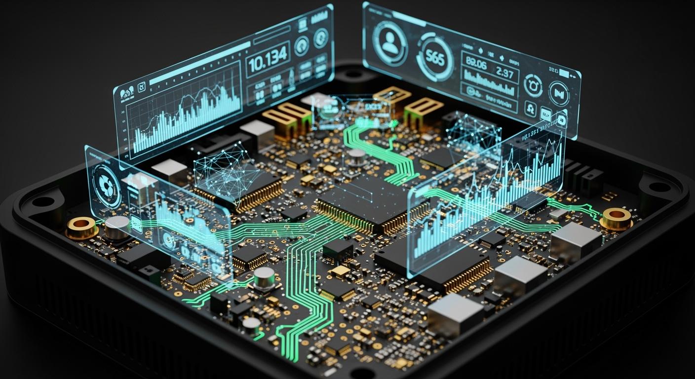
How HDI PCB Technology Enhances Device Miniaturization
You see smaller and smarter devices every day because of HDI PCB Technology. This technology uses special via structures like blind, buried, and micro vias. These help fit more parts into a smaller space. Because of this, makers can make devices up to 60% smaller than before. Many electronics, like smartphones and wearables, use these small, high-density boards. They need them to work well and last a long time.
Key Takeaways
HDI PCB Technology helps make devices smaller. It uses special via structures. This can make electronics up to 60% smaller. Microvias and fine line routing help signals stay strong. They also cut down on interference. This makes devices faster and more reliable. Using fewer layers in circuit boards saves money. It also makes the design easier. Production becomes more efficient. Miniaturization boosts how well devices work. It lets devices have more features in small designs. These devices use less power. HDI PCBs are very important in modern electronics. They are used in things like smartphones and medical devices. This makes them light and efficient.
HDI PCB Technology Features
Micro Vias and Via Structures
You can fit more parts into a small space when you use special via structures. Blind vias connect the outer layers of a circuit board to one or more inner layers. They do not go through the whole board. This design helps you reduce the size and complexity of your board. Buried vias connect only the inner layers. They never reach the surface. This feature lets you place more components on the outside and keep signals safe from noise. Microvias are even smaller than regular vias. They make it possible to create high-density interconnections. You see these in compact devices like smartphones and IoT gadgets. Microvias also help keep signals strong and clear. They reduce the length of signal paths and lower the chance of signal loss or interference.
Tip: Using buried vias can help you avoid signal problems and keep your device working well.
Fine Line Routing
Fine line routing lets you draw very thin lines and put them close together on your board. With HDI PCB Technology, you can make traces as narrow as 30 microns. Some advanced factories can even go down to 25 microns. This means you can fit more connections in a smaller space. You need to design these lines carefully. If you make them too thin, you might get defects or lose signals. Fine line routing helps you keep your board small and light. It also supports high-speed signals by making the paths shorter and more direct.
High Component Density
You can add more parts to your board when you use HDI PCB Technology. This technology supports a high component density. It uses microvias and tight routing to fit many connections in a small area. You can place chips with many pins and small gaps between them. This is important for modern electronics, where space is limited. Shorter signal paths also mean better signal quality and less power loss. You get a board that works better and lasts longer.
HDI PCBs support very concentrated routing.
You can use advanced chips like BGAs with many pins.
Microvias help you save space and improve signal strength.
When you use these features, you make your devices smaller, faster, and more reliable.
Miniaturization Mechanisms
Space Optimization
HDI PCB Technology helps make devices smaller and lighter. You can design boards that are complex but still compact. You do not lose important features. Microvias are tiny holes that connect layers and save space. They are 0.1 mm or less in diameter. Thin traces, sometimes only 50-75 micrometers wide, fit more circuits in a small area. These tricks let you pack more functions into less space.
Microvias, fine lines, and lamination steps add more features.
Your board can be up to 50% smaller and lighter than old designs.
Lower resistance, capacitance, and inductance help use a smaller battery.
Note: Smaller boards make devices easier to carry and use.
Layer Reduction
You can use fewer layers in your circuit board. This saves money and makes your board work better. For example, you might go from 8 layers to just 4 layers. Fewer layers mean less material and less time to make each board.
Standard PCB Layers | HDI PCB Layers |
|---|---|
12 | 8 |
Aspect | Impact on Costs and Performance |
|---|---|
Layer Reduction | Lowers material and production costs |
Performance Improvement | Enhances signal integrity and reduces design complexity |
Cost-Effectiveness | A single HDI PCB can replace multiple traditional PCBs |
You save money by using fewer materials.
Your board is simpler and easier to design.
One new board can replace several old boards.
You might pay more at first to start making boards.
The cost per board goes down as you make more.
Special tools cost less when used for many boards.
Signal Integrity
HDI PCB Technology keeps signals strong and clear. Parts are closer together, so signal paths are shorter. This helps avoid signal loss and crosstalk. Microvias and fine traces reduce signal reflections and keep data safe, even at high speeds.
Advanced interconnections like microvias and through-silicon vias help with complex circuits.
Components are closer, which shortens signal paths and improves quality.
Laser drilling makes microvias and helps reduce signal delays.
Any-layer via technology gives higher circuit density and better performance.
HDI PCB Technology lets you build smaller, faster, and more reliable devices. You get better signal quality, less interference, and more features in a small space.
Applications of HDI PCB Technology
Consumer Electronics
Many devices you use every day need HDI PCB Technology. Smartphones, smartwatches, and tablets all use small, strong circuit boards. These boards help make phones thin but still have big screens and long battery life. Smartwatches and fitness trackers use HDI PCBs to fit sensors, chips, and batteries into tiny cases. This technology also helps thin laptops stay light and work fast.
Device Type | Application of HDI PCB Technology |
|---|---|
Smartphones | Use of ELIC HDI constructions for compact designs |
Wearables | Integration in smartwatches, fitness trackers, VR/AR headsets for sleek profiles and dense sensor integration |
Tablets | Dependence on HDI for high processing power and extended battery life |
Thin Laptops | Utilization of HDI for maintaining slim profiles while enhancing performance |
People want smaller and better devices, so companies add more features to tiny gadgets.
Most new smartphones use HDI boards with 6-10 layers.
Smartwatches need HDI PCBs for cool features in small spaces.
Medical Devices
Medical devices help keep you healthy and safe. HDI PCB Technology makes these devices smaller and more dependable. Doctors use small monitors, hearing aids, and devices inside the body that need this technology. Smaller circuit boards mean tools are less invasive and patients heal faster.
HDI PCBs help make medical devices tiny.
They make devices work better, which keeps patients safe.
Advanced sensors and real-time checks give better results.
In things like pacemakers, HDI PCBs make sure the device is small and works well for a long time.
Automotive and IoT
You find HDI PCB Technology in cars and smart devices at home. New cars use small control units, sensors, and entertainment systems. These parts must fit in small spaces and move lots of data fast. HDI PCBs help by making wiring tighter and boards smaller.
Car electronics use HDI PCBs for smart features and fast data.
IoT devices, like smart home sensors, need small boards to fit anywhere and use little power.
HDI PCB Technology helps shrink car sensors and smart gadgets, making your world smarter and more connected.
Miniaturization Benefits
Performance Enhancement
Miniaturized boards help devices work better. HDI PCB Technology lets you put more parts in a small space. This means your device can do more things at once. Shorter signal paths make signals move faster. They also lower resistance and other problems. Your device uses less voltage and current. This keeps it cool and lets you use smaller batteries. Finer lines and tiny vias let you add chips with lots of pins. This is important for new devices that need speed and power. You can make your device much smaller and still keep all its features.
Tip: Faster circuits and clearer signals help your device run well, even when it is small.
Reliability Improvement
Miniaturized devices are strong and dependable. HDI PCB Technology uses special materials and careful steps to build boards. This makes your board tough and reliable. Fewer layers and fewer solder joints mean fewer things can break. Microvias make the board stronger. Your device can handle heat, shaking, and cold or hot weather. Some boards work from -40°C to 85°C. In space, they can go from -150°C to +120°C. This reliability is important for medical devices, cars, and planes, where safety matters.
HDI PCBs last longer in rough places.
You see fewer problems because there are fewer weak spots.
Devices like pacemakers and sensors stay safe and steady.
Cost Efficiency
Miniaturized boards help you save money. HDI PCB Technology lets you fit more parts on each board. You use less material. When you make lots of boards, your cost per board goes down. You waste less and build boards faster. Even if you pay more at first, you spend less later. You use fewer materials and need less work.
Key Cost Savings | Explanation |
|---|---|
Lower cost per unit in big orders | You can save up to 40% when you make lots of boards. |
Material optimization | Smaller boards use less material, which cuts costs. |
Faster production | Less waste and quick prototyping save time and money. |
Long-term savings | Over time, you spend less because of better efficiency and less labor. |
Miniaturization lets you make smaller phones, smarter wearables, and better medical tools. You also get ahead by making devices that are lighter, faster, and use less energy.
You can see that HDI PCB Technology helps make devices smaller. This technology lets you use thinner boards. You can also put parts inside the board. You can place components closer together. Here are the main benefits:
Benefit | What It Means for You |
|---|---|
Space Reduction | Fit more parts in less space for smaller devices |
Save space and lower weight by putting parts in the board | |
Advanced Methods | Use new tools for better, more compact designs |
You get products that are faster and more reliable. They also cost less to make. Try using these ideas when you design your next small device.
FAQ
What is HDI PCB Technology?
HDI PCB Technology lets you put more parts on a board. It uses tiny vias and thin lines. This helps make devices smaller and smarter.
Why do you need microvias in HDI PCBs?
Microvias connect layers but do not use much space. You can add more parts and keep signals strong. Devices work better and last longer.
How does HDI PCB Technology improve device reliability?
You get stronger boards with fewer weak spots. HDI PCBs can handle heat, shaking, and hard use. Devices stay safe and steady.
Can you use HDI PCBs in medical devices?
Yes! HDI PCBs are used in medical devices like pacemakers and hearing aids. These boards make devices smaller and more reliable.
What are the main benefits of device miniaturization?
You save space and lower costs. Devices get lighter, faster, and easier to carry. You also get more features in a small device.
See Also
Combining SMT And DIP Techniques For Superior PCB Performance
Essential Guidelines For HDI PCB Surface Mount Assembly
DIP PCBA Production: Process, Quality Assurance, And Uses
Improving PCB Production Efficiency Through EMS Company Strategies