Environmental Stress Screening keeps your PCBA safe and sound
Imagine your electronics stop working when you need them most. Environmental stress screening helps protect your PCBA. It finds hidden problems before products go to customers. Studies show hidden solder problems, like voids in BGA joints, often cause failures and warranty claims.
Industry groups say missed manufacturing problems are a top reason for PCBA failure.
These problems can hurt your reputation and make things cost more.
You can see how ESS helps in the table below:
Cost Category | Without ESS | With ESS |
|---|---|---|
ESS Equipment (amortized) | $0 | $15-50 per unit |
Field Service Call | $500-2000 | Avoided |
Warranty Replacement | Full unit cost | Avoided |
Customer Dissatisfaction | Lost future sales | Maintained reputation |
Recall Risk | Potential liability | Greatly reduced |
Environmental stress screening helps you feel calm. It finds problems early and keeps your PCBA safe.
Key Takeaways
Environmental Stress Screening (ESS) finds hidden problems in PCBAs before customers get them. This makes the product more reliable.
Using ESS lowers the number of failures a lot. This means there are fewer warranty claims and repair costs go down.
Starting ESS early in making products helps keep quality high. It also keeps customers happy.
Check and change your ESS program often. This makes sure it finds weak boards but does not hurt good ones.
Use different stressors like temperature and humidity in your ESS. This helps find many types of problems.
What is Environmental Stress Screening?
ESS Definition
You need to understand what environmental stress screening does for your PCB assembly. Environmental stress screening, or ESS, uses things like temperature and humidity to find hidden problems in your PCB. This process happens during manufacturing. Highly Accelerated Stress Screening, called HASS, puts these stresses on your PCB assembly. This method helps you find defects that might show up later. You can catch issues before your product leaves the factory.
Environmental stress screening looks at two main stressors: temperature and humidity. These stressors help you find weak spots in your PCB assembly. Different stress profiles target certain failure mechanisms. You can see them in the table below:
Failure Mechanism | Effective ESS Stress | Typical Profile |
|---|---|---|
Solder joint crack (thermal fatigue) | Thermal cycling (rapid ramp) | -20/+85°C, 15°C/min, 50 cycles |
CAF / Electrochemical migration | Temperature‑humidity‑bias (THB) | 85°C/85% RH, 50V bias, 96h |
Component infant mortality (ICs) | Burn‑in (elevated temperature + power) | 125°C, 48h, powered with pattern |
You use environmental stress screening to find manufacturing defects that regular inspection might miss. These defects include cold solder joints, solder bridges, and cracked ceramics. You can see common defects and how ESS finds them in the table below:
Defect Type | Description | ESS Detection Method |
|---|---|---|
Cold Solder Joint | Rough, grainy joint from not enough heat | Temperature cycling makes cracks grow |
Solder Bridge | Unwanted connection between nearby pads | Thermal expansion shows short circuits |
Insufficient Solder | Joint with weak bond because not enough solder | Vibration and thermal stress cause opens |
Cracked Solder | Breaks in solder material | Temperature cycling makes cracks bigger |
Head-in-Pillow (BGA) | BGA ball touches but doesn’t stick well | Combined stress shows bad connections |
Marginal Capacitors | Weak or out-of-spec dielectric | Temperature and voltage cycling cause breakdown |
Contaminated ICs | Moisture or particles inside | Humidity and temperature show leakage |
Cracked Ceramics | Tiny cracks in ceramic packages | Thermal shock makes cracks worse |
Weak Wire Bonds | Bad chip connections inside | Temperature cycling and vibration cause opens |
Loose Connectors | Not fully seated or partly connected | Vibration shows bad connections |
Missing Hardware | Screws, washers, or fasteners not there | Vibration causes mechanical failures |
Damaged PCB Traces | Scratches or cracks in copper traces | Thermal stress opens damaged traces |
Lifted Pads | Pad comes off PCB base | Temperature cycling finishes separation |
Tip: You can use environmental stress screening to find these defects early. This step helps you avoid expensive repairs and keeps your PCB assembly reliable.
Purpose for PCBA
You want your PCB assembly to work every time. Environmental stress screening helps you reach this goal. You use ESS to find defects from manufacturing. These defects may not show up during basic inspection. You can stop failures by stressing your PCB assembly before it goes to your customer.
Environmental stress screening does not replace reliability testing. Reliability testing checks if your PCB works under normal conditions. ESS pushes your PCB assembly past normal limits. This process helps you find hidden defects and weak spots. You can see the difference in the table below:
Testing Method | Purpose |
|---|---|
Traditional Reliability Testing | Checks performance under normal conditions. |
Environmental Stress Screening | Puts PCBs through different conditions to find hidden defects and speed up aging. |
Thermal Cycling | Tests if PCB can handle fast temperature changes like real-world environments. |
You use environmental stress screening with reliability testing. This gives you the best chance to deliver a safe and sound PCB assembly. You protect your product and your reputation.
Why ESS Matters for PCBA Reliability
Common PCBA Risks
You want your pcb assembly to work every time. There are many risks that can make your pcb fail. Most of these risks come from problems made during manufacturing. You cannot always see these problems right away. If you do not use environmental stress screening, you might have trouble later.
Here are some common risks you should know:
Failure Mode | Symptoms | Causes | Solutions |
|---|---|---|---|
Poor Electrical Performance | Unstable circuit functionality or substandard performance. | Mismatched component parameters, improper PCB design. | Ensure component parameters meet design specifications, optimize PCB design. |
Insufficient Cleaning | Residual flux, dust, or contaminants. | Incomplete cleaning process, use of substandard cleaning agents. | Optimize cleaning process, use qualified cleaning agents. |
Mechanical Damage | Scratches or detached components. | Improper handling during assembly or transportation. | Provide operator training, implement protective measures. |
Failure under extreme conditions. | Inadequate environmental stress resistance of components. | Select components with strong resistance, conduct Environmental Stress Screening tests. | |
Software or Firmware Issues | Abnormal functionality due to software issues. | Software bugs, incorrect programming. | Strengthen software testing, verify firmware flashing. |
Improper Copper Weight | Issues due to incorrect copper sizing. | Copper too thin or thick, incorrect sizing during layout design. | Adhere to copper weight specifications, avoid excessive thickness. |
Many failures happen because of small mistakes in manufacturing. These problems can make your pcb assembly stop working. Sometimes it may act in strange ways. You need to find these risks early to keep your product safe.
How ESS Reduces Failures
You can use ess to find hidden problems before shipping. Environmental stress screening puts your pcb assembly through tough tests. These tests use heat and humidity. This helps you find weak spots and remove bad boards.
When you use ess, you lower the number of failures. The table below shows how much reliability improves:
Metric | Value Before ESS | Value After ESS | Reduction |
|---|---|---|---|
Failure Rate | 2.8% | 0.4% | 2.4% (approx. 86% reduction) |
Cost of ESS per Board | N/A | $12 | N/A |
Estimated Savings per Board | N/A | $50 | N/A |
You can see that ess drops the failure rate from 2.8% to 0.4%. This means your pcb is more reliable and you get fewer returns. You also save money because you do not need as many repairs. By using ess, you help your pcb assembly stay safe and sound.
Tip: You can trust ess to find problems that normal tests might miss. This step helps you feel calm and lets you deliver good products.
ESS Process Overview
Typical Steps
You can use a simple process for ess in manufacturing. This process helps you find and fix problems before customers get your product. Here are the main steps you should follow:
Put your PCBA through environmental stresses. This helps you find problems that normal tests might miss.
Test every board one by one. You do not want to miss any weak boards.
Use different stress profiles like temperature cycles or vibration. These profiles copy real-world conditions and push your boards hard.
Check your boards after screening. You can see how much your ess program helps your product.
You can do these steps for each batch you make. This helps you find problems early and saves money on repairs. Many companies use halt and hass with ess. Halt means Highly Accelerated Life Test. You use halt to find out how much stress your design can take. Hass, or Highly Accelerated Stress Screening, helps you find weak boards during manufacturing. You can use these methods together to make your ess program even better.
Tip: You can use halt to pick the right stress levels for your ess. This helps you find problems without breaking good boards.
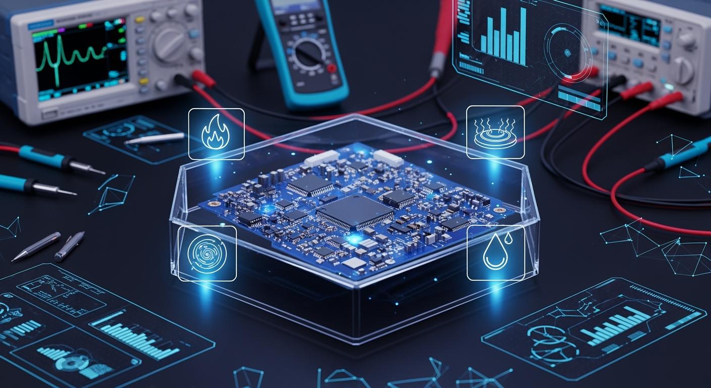
Environmental Stressors Used
You can use different stressors in your ess program. The most common ones are temperature, humidity, and vibration. Each stressor helps you find different types of problems. You can see what each stressor does in the table below:
Stressor | What It Does | Common Defects Found |
|---|---|---|
Temperature | Heats up and cools down your board | Solder cracks, lifted pads |
Humidity | Adds moisture to the environment | Contaminated ICs, corrosion |
Vibration | Shakes the board | Loose connectors, weak bonds |
You can use hass to mix these stressors. This makes your ess program work better. You can also use halt to test how strong your design is before you start making products. Many companies use highly accelerated life test to make sure their products last longer.
You can change the stress levels to fit your product. This helps you find problems but keeps your boards safe. When you use ess with halt and hass, you protect your PCBA during manufacturing.
Benefits of Environmental Stress Screening
Early Defect Detection
You want to find problems in your pcb before customers get them. ESS helps you catch defects early during manufacturing. Regular inspections check design and durability. ESS does more. You can find hidden issues like weak solder joints or loose connectors right after assembly. This early detection lets you fix problems before they cause failures. You improve quality and lower the risk of sending out bad boards.
Tip: If you find problems early, you can fix them fast. This keeps your production line working well.
Improved Reliability
You need your pcb assembly to work every time. ESS helps you reach this goal. Stress tests like temperature cycling and vibration find weak spots that normal checks miss. Removing weak boards makes your products more reliable. Customers trust your brand more when your pcb assembly works well. You avoid costly failures that can hurt your reputation.
Here is how ESS helps reliability:
Takes out boards with hidden defects
Lowers the number of failures in the field
Makes customers happier
Cost and Warranty Savings
You want to save money and protect your business. ESS lowers costs by reducing failures and warranty claims. Catching problems early helps you avoid expensive repairs and replacements. You spend less on customer support and field service calls. This means you can put more money into quality and less into fixing mistakes.
Cost Area | Without ESS | With ESS |
|---|---|---|
Warranty Claims | High | Low |
Field Repairs | Frequent | Rare |
Customer Complaints | Many | Few |
Quality Control | Reactive | Proactive |
You get better quality, fewer failures, and more savings when you use environmental stress screening in your manufacturing process.
ESS Implementation Tips
Best Practices
You want your ess program to work well every time. Start by planning your ess program before you begin manufacturing. Set clear goals for what you want to find. Choose stress levels that match your pcb design. Use data from past failures to guide your choices. Test a small batch first. This helps you see if your ess program finds weak boards.
You should monitor each step. Keep records of every pcb that goes through the ess program. Track which boards fail and why. Use this information to improve your process. Train your team to spot signs of failure during screening. Make sure everyone knows how to handle the equipment safely.
Tip: Review your ess program results often. Adjust your stress levels if you see too many or too few failures.
Overcoming Challenges
You may face some problems when you add an ess program to your manufacturing line. Sometimes, you might worry about damaging good boards. To avoid this, use halt to set safe stress limits for your pcb. If you see too many failures, check your process for mistakes. Look for issues in soldering, cleaning, or handling.
You might also find it hard to fit the ess program into your schedule. Plan your screening steps so they do not slow down production. Use clear checklists to keep things moving. If you have trouble with equipment, keep spare parts ready and train your team to fix small problems.
Challenge | Solution |
|---|---|
Too many failures | Check process, adjust stress |
Damaged good boards | Use halt to set safe limits |
Slow production | Plan steps, use checklists |
Equipment issues | Train team, keep spares handy |
You can make your ess program strong by learning from each batch. Keep improving your process to protect every pcb and boost reliability.
You can use ESS to help your PCBA stay safe. This process finds hidden problems that regular checks miss. It makes your boards work better and last longer. You save money because you fix issues early. Your reputation stays strong and your customers stay happy. Make ESS part of your quality plan. Start using ESS now and your products will work better soon.
Remember: Good products start with smart screening.
FAQ
What is Environmental Stress Screening?
You use Environmental Stress Screening to test your PCBA with heat, humidity, and vibration. This process finds hidden defects before your product reaches customers. ESS helps you make your boards safer and more reliable.
How often should you run ESS on your PCBA?
You should run ESS on every batch during manufacturing. This step helps you catch problems early. If you change your design or process, you need to update your ESS plan.
Does ESS damage good boards?
You set safe stress levels using HALT. This keeps good boards safe. ESS only removes weak boards. You protect your product by finding the right balance.
What equipment do you need for ESS?
You need chambers for temperature and humidity, vibration tables, and test tools. You can use simple setups or advanced machines. Choose equipment that fits your product and budget.
Can ESS lower warranty costs?
Yes! ESS finds defects before shipping. You avoid costly repairs and replacements. Your warranty claims drop, and you save money.
See Also
Understanding PCBA Processing Needs for Medical Devices
The Impact of X-Ray Inspection on PCBA Quality Assurance
The Importance of Aging Tests for PCBA Products
Significance of SPI Inspection Post-SMT in PCBA Production
Essential Strategies for Enhancing PCBA Reliability Over Time