Emerging Trends Shaping the SMT PCBA Process in 2025
As technology continues to advance and the demand for printed circuit boards rises, the smt pcba process is experiencing rapid transformation. Automation, AI, and miniaturization are driving significant changes in both manufacturing and design. The printed circuit board industry is adapting to these shifts by implementing innovative strategies. The table below highlights key projected trends for 2025 related to the smt pcba process:
Trend Description | Projected Value/Share |
|---|---|
Global PCB market growth | |
Market size for 8-16 layer PCBs | $45B by 2025 |
Cost increase in copper | 15% increase in 2025 |
China's share of global production | 50% by 2025 |
Key Takeaways
Embrace automation in PCB production to enhance efficiency and reduce errors. Smart robotics and AI systems can significantly speed up manufacturing processes.
Stay updated on miniaturization trends. Smaller components allow for more compact and powerful devices, which is essential for meeting market demands.
Adopt sustainable practices in PCB manufacturing. Using eco-friendly materials and energy-efficient processes not only benefits the environment but also improves your brand's reputation.
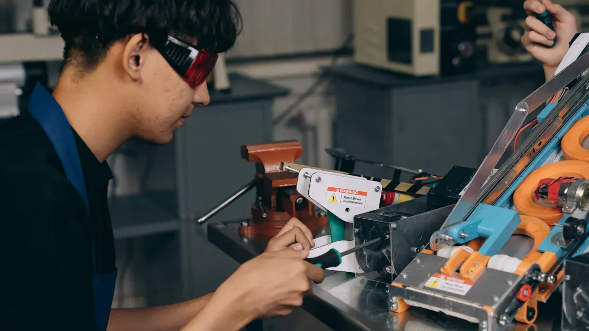
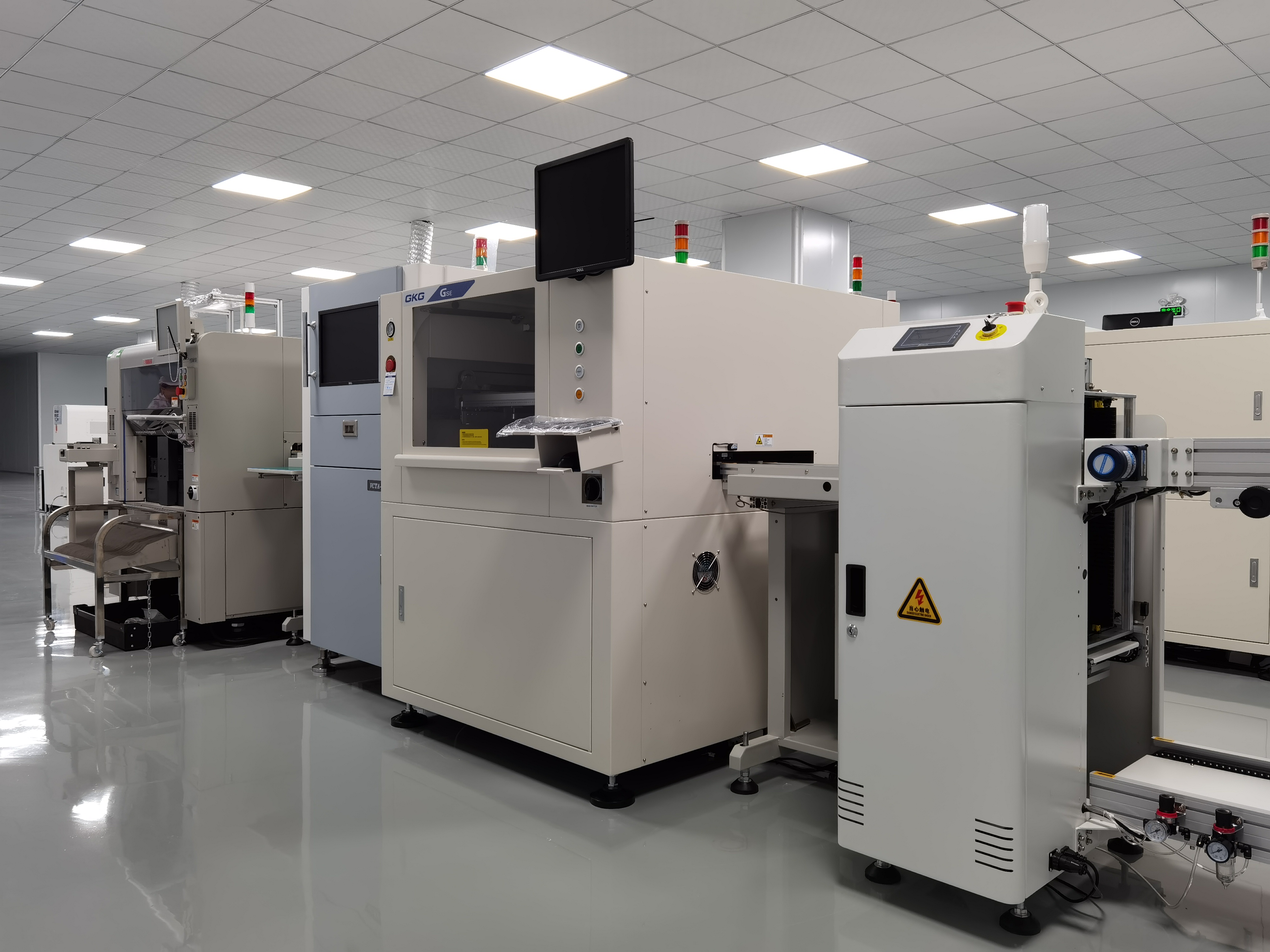
Automation In SMT PCBA Process
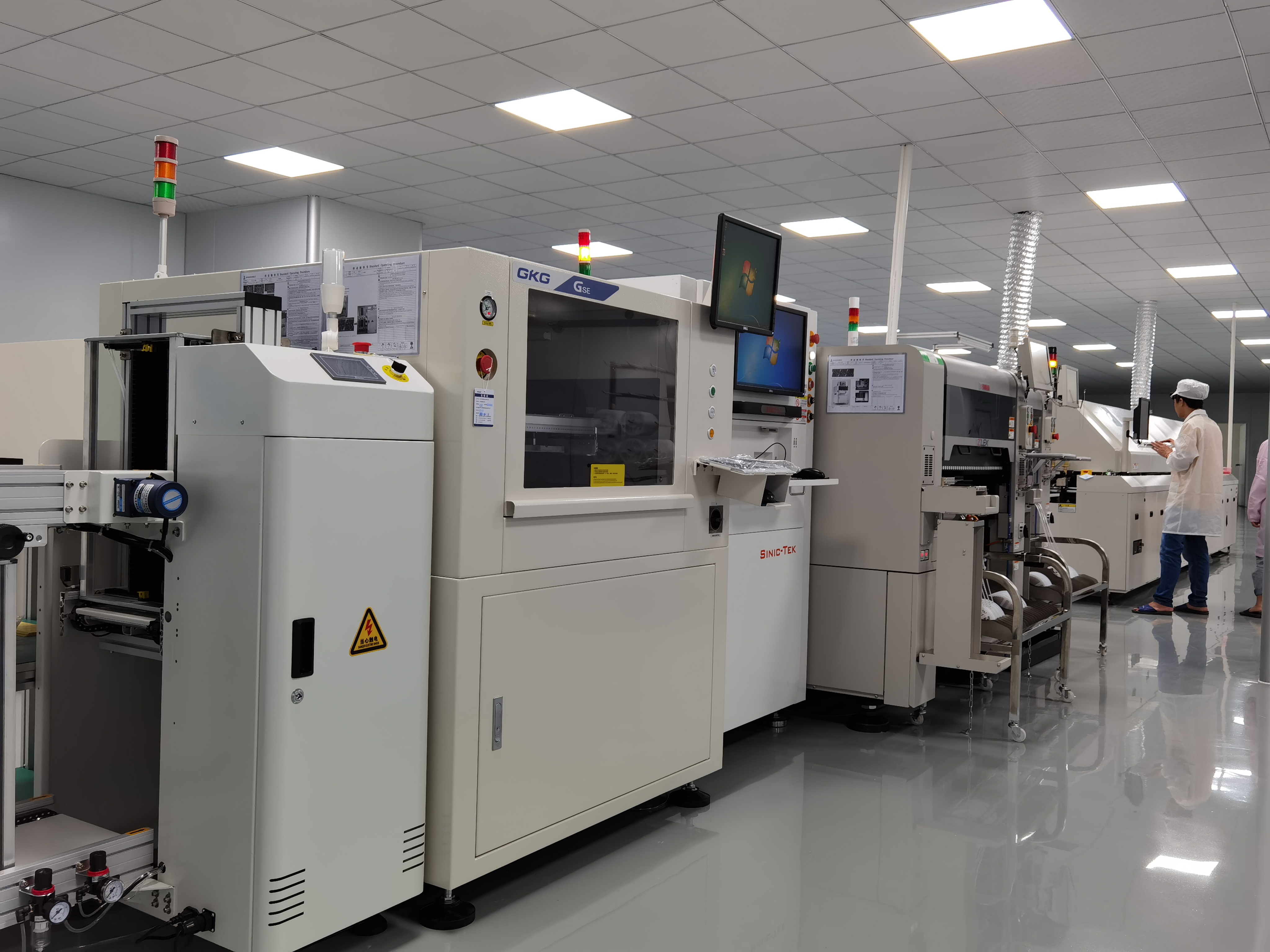
Automation in pcb production is changing how you approach the smt pcba process. You see faster production cycles and improved quality control. Industry 4.0 brings smart robotics and AI-powered vision systems into your assembly lines. These technologies help you meet rising demand and adapt to new trends in surface mount technology.
The integration of automated pcb assembly offers numerous advantages that contribute to improved manufacturing outcomes, including enhanced precision, increased efficiency, and reduced human error.
AI-Powered Vision Systems
AI-powered vision systems now play a key role in smt processes. You can detect defects as small as 0.025 mm. Real-time data analysis lets you catch problems early, which reduces waste and improves quality. These systems lower false alarms, so only defective boards need inspection. LTPCBA uses advanced automated systems to ensure consistent quality in every pcb assembly.
Smart Robotics
Smart robotics drive automation and robotics in modern assembly. Robots perform repetitive tasks with high precision, reducing human error in smt processes. You benefit from continuous operation, which increases throughput and lowers labor costs. Automated systems adjust quickly for different product lines, giving you flexibility and scalability. LTPCBA’s quick response service and 24-hour support help you keep up with industry 4.0 and changing market needs.
Benefit | Description |
|---|---|
Enhanced Efficiency | Automation increases production speed, allowing manufacturers to meet high demand without compromising quality. Machines work continuously, reducing downtime and cycle times. |
Consistent Quality | Automated systems improve product quality consistency, reducing human error and ensuring high precision in repetitive tasks. |
Cost Savings | Long-term savings on labor and waste reduction can lead to increased profit margins despite initial investment costs. |
Flexibility and Scalability | Automated systems can be adjusted for different product lines, essential for adapting to market changes. |
You see automation in pcb production and industry 4.0 making assembly faster, smarter, and more reliable. LTPCBA leads the way with advanced technology and a commitment to quality in every pcb assembly.
Miniaturization Trends
Miniaturization trends shape the future of electronics. You see devices getting smaller and more powerful every year. This shift changes how you design and manufacture printed circuit boards. As demand for compact products grows, you must adapt to new technology and assembly methods.
Component Size Reduction
You notice that electronic components keep shrinking. Smaller chips and resistors allow you to fit more features into less space. This trend lets you create thinner smartphones, lighter wearables, and smarter devices. Miniaturization trends push you to use advanced placement machines and precise soldering techniques. You must pay close attention to spacing and alignment. Even a tiny error can affect performance. As you work with smaller parts, you improve your skills and use better tools.
High-Density PCB Assembly
Miniaturization and high-density interconnects go hand in hand. You pack more circuits onto each board. This approach increases complexity, but it also boosts performance. The complexity index helps you measure how hard it is to build these boards. It affects your first pass yield, which shows how many boards pass inspection the first time. When you use a one-stop manufacturing process, you often see higher yield rates. You can spot and fix problems early, which keeps quality high.
High-density PCB assembly brings challenges:
Defect rates can rise if you do not control the process.
Quality control becomes even more important.
Miniaturization trends will keep driving innovation. You must stay updated on the latest technology to meet the growing demand for smaller, smarter products.
Flexible And Wearable Electronics
The rise of flexible and wearable electronics marks one of the most important trends in the SMT PCBA process. You see growing demand for devices that bend, stretch, and fit seamlessly into daily life. This shift pushes you to adopt new technology and rethink how you design and assemble products. Market growth is strong in several regions:
Europe leads with automotive innovation, especially in Germany and Italy, where vehicles now use flexible and stretchable pcbs.
North America experiences rapid growth as consumers want more wearables and smart devices.
The Middle East & Africa invest in smart city projects, using flexible and stretchable pcbs for healthcare wearables.
Stretchable PCBs
You face unique challenges when working with flexible and stretchable pcbs. Achieving a conformal fit and ensuring reliability under repeated stress are top concerns. You can solve these issues by using wider traces, reinforcing high-stress areas, and selecting materials like polyimide for flexibility and thermal stability. Polyimide and rolled annealed copper help flexible pcbs maintain their shape during bending and stretching. Engineers also use high-density interconnect PCBs and smaller surface-mount components to save space. Effective power management, such as using low-power components and optimizing layouts, extends battery life in wearable devices.
Compact Device Integration
Compact device integration changes how you approach SMT PCBA design. You use advanced packaging and high-density interconnect technology to fit more features into smaller spaces. The table below shows how these solutions impact your work:
Evidence Description | Impact on Design and Assembly |
|---|---|
Miniaturization through advanced packaging technologies (CSPs, WLP, etc.) | Enables higher component densities and more advanced product designs, crucial for compact device integration. |
3D packaging solutions (TSV technology) | Reduces package footprint and improves signal integrity, enhancing performance in compact designs. |
High-density interconnect technologies (embedded trace substrates, FO-WLP) | Facilitates integration of more functionality within a smaller footprint, essential for modern SMT PCBA products. |
Flexible pcbs and flexible and stretchable pcbs now play a vital role in meeting the demand for smaller, smarter, and more adaptable electronics.
Sustainability In PCB Manufacturing
You see sustainability becoming a top priority in pcb manufacturing. As the demand for eco-friendly products grows, you must adopt sustainable practices in every step of the smt pcba process. These trends shape how you select materials, manage energy, and design high-quality rigid flex pcb manufacturing. LTPCBA leads the way by following international standards and focusing on sustainability and green manufacturing.
Green Materials
You can make a big impact by choosing green materials in pcb manufacturing. These options help you reduce waste and protect the environment. Here are some of the most widely used green materials:
Biodegradable substrates break down naturally, so they lower landfill waste.
Eco-friendly coatings cut toxic emissions and create a safer workplace.
Water-based inks reduce air pollution by minimizing VOC emissions.
When you use these materials in pcb assembly, you support sustainable practices and improve the overall quality of your pcba.
Energy Efficiency
Energy efficiency is another key part of sustainability in pcb manufacturing. You can save money and help the planet by using less energy and recycling materials. The table below shows how energy-efficient practices benefit your business and the environment:
Aspect | Benefit |
|---|---|
Cost Savings | Lower energy use and less material waste mean you spend less over time. |
Environmental Impact | Cutting carbon emissions and waste helps fight climate change. |
Sustainable Practices | Recycling copper and using efficient processes lower production costs. |
You see that sustainable practices and high-quality rigid flex pcb manufacturing go hand in hand. By focusing on sustainability, you meet new industry standards and build trust with your customers. LTPCBA’s commitment to quality and sustainability ensures you get reliable pcb assembly that meets global expectations.
Advanced Materials And Wafer Technology
You see advanced materials and wafer technology changing the way you approach pcb manufacturing. The demand for smaller, faster, and more reliable devices pushes you to explore new solutions. You work with advanced smd components that require precise handling and innovative materials. The table below highlights key advancements shaping pcb manufacturing in 2025:
Advancement Type | Description |
|---|---|
High-Density Interconnect (HDI) | Finer lines and smaller vias boost functionality in compact designs, perfect for advanced smd components. |
Flexible and Stretchable PCBs | Enable products that bend and conform, supporting advanced smd components in wearables and sensors. |
Specialized materials like PTFE ensure signal integrity for advanced smd components in 5G and automotive applications. | |
Embedded Component Technology | Embeds advanced smd components within pcb layers, improving performance and reducing size. |
Rapid prototyping and customization of pcb manufacturing, ideal for unique advanced smd components. |
300 mm Wafer Transition
You notice the transition to 300 mm wafers in pcb manufacturing brings major benefits and challenges. You produce more chips per wafer, which lowers cost per die and increases efficiency. Automation in manufacturing boosts yield and reduces labor costs. You face challenges such as higher capital investment and increased complexity in handling larger wafers. You must control defects carefully because the larger surface area can amplify issues. The table below summarizes these points:
Benefit/Challenge | Description |
|---|---|
Lower Cost per Die | More chips from each wafer reduce costs in pcb manufacturing. |
Improved Efficiency | Automation increases yield for advanced smd components. |
Capital Investment | Upgrading facilities for 300 mm wafers requires significant resources. |
Handling Complexity | Larger wafers need careful processing to avoid defects in advanced smd components. |
Lead-Free Solder
You respond to global regulations by using lead-free solder in pcb manufacturing. This change supports environmental safety and meets RoHS directives. You select solder pastes with low melting points and strong mechanical properties to maintain reliability for advanced smd components. Lead-free solder can be less ductile, so you pay close attention to stress conditions in your pcb designs. You ensure compliance and product reliability by choosing the right materials for advanced smd components.
You meet demand for safer products in pcb manufacturing.
You maintain reliability for advanced smd components by selecting quality solder pastes.
Predictive Analytics In PCBA
Design Optimization
You can use predictive analytics to transform your approach to design optimization in the SMT PCBA process. This technology helps you analyze large sets of historical data and market trends. You can forecast demand and adjust your procurement strategies before production even begins. When you use predictive analytics, you make smarter decisions about component selection and layout. This leads to better optimization of your designs and reduces costly revisions.
Automated PCB inspection powered by predictive analytics not only detects defects but also acts as a predictive quality assurance system.
Predictive analytics enhances design efficiency by analyzing past data and market trends, allowing you to forecast demand and optimize procurement.
AI-driven predictive analytics in quality assurance can forecast potential failures before products leave your facility, which improves overall product quality.
You see that design optimization becomes more efficient and accurate when you rely on data-driven insights. This approach helps you stay ahead of the competition and meet the growing demand for smarter electronics.
Reliability Improvements
Reliability is critical in every PCBA project. Predictive analytics gives you the tools to identify risks before they become problems. You can use predictive models based on SPI parametric data to spot potential ICT defects early in the process. This level of optimization means you can prevent failures and deliver more reliable products.
Evidence Description | Precision Score | Implication |
|---|---|---|
Predictive models based on SPI parametric data can predict ICT defects | > 82% | Helps in making informed decisions to prevent defects, improving reliability |
You gain confidence in your process when you use predictive analytics for reliability improvements. This technology supports your optimization goals and ensures your products meet high standards every time.
IoT Integration In PCB Assembly
Smarter Devices
You see IoT integration changing how you design and use electronic devices. Devices now collect data, connect to networks, and respond to your needs in real time. This integration leads to smarter devices that improve your daily life and business operations. You can control and monitor equipment remotely, which saves time and increases efficiency. Predictive maintenance helps you avoid costly breakdowns by fixing problems before they grow. Automation reduces errors and speeds up processes. Smart devices also adjust settings based on your preferences, making your experience more comfortable and secure.
Mechanism | Impact on User Experience and Operational Efficiency |
|---|---|
Enables real-time tracking and management of devices, enhancing operational agility and convenience. | |
Proactive Maintenance | Predictive analytics prevent issues before they escalate, increasing equipment uptime and reducing costs. |
Automation | Reduces human intervention, minimizing errors and waste, thus improving operational precision and speed. |
Increased Convenience and Comfort | Intelligent settings adjust automatically to user preferences, enhancing comfort and security in operations. |
Data-Driven Decision-Making | Provides real-time insights for evidence-based strategies, improving workflows and giving a competitive advantage. |
You notice the demand for smarter devices continues to rise as more industries adopt IoT technology.
Connectivity Solutions
You need strong connectivity solutions to support IoT integration in PCB assembly. Materials like PTFE and Rogers RO4000 Series help reduce signal loss and improve stability for high-frequency applications. Hybrid stack-ups combine cost savings with efficient performance, making them ideal for mass production. You use HDI PCBs to fit more features into smaller spaces. RF shielding layers protect signals from outside interference, and controlled impedance design keeps signals clear and reliable.
HDI PCBs allow compact designs with microvias and fine-pitch components.
RF shielding layers block interference and maintain signal quality.
Controlled impedance design ensures consistent performance.
You see that successful integration of these solutions supports the growing technology needs of IoT devices.
Quality Assurance In PCBA
Automated Optical Inspection
You rely on automated optical inspection to keep your assembly process accurate and efficient. This technology has changed how you approach pcb manufacturing. High-resolution imaging systems now capture even the smallest details on every pcb. You spot defects early, which helps you meet the demand for flawless products. Innovative illumination, such as conical convergence technology, creates bright areas that remove blind spots. You see every part of the assembly, so nothing gets missed. AI and machine learning now play a big role in automated pcba. These tools boost inspection accuracy and allow real-time defect detection. You can even predict when maintenance is needed, which keeps your assembly lines running smoothly.
Advancement Type | Description |
|---|---|
High-resolution imaging | Systems deliver exceptional low-noise performance, capturing even the smallest details with clarity. |
Innovative illumination | Conical convergence technology creates a high-brightness area, eliminating blind spots for defect detection. |
AI and machine learning | Integration enhances inspection accuracy and enables real-time defect detection and predictive maintenance. |
You use these advancements to improve every step of pcb manufacturing. Your assembly process becomes faster and more reliable.
LTPCBA's Quality Standards
You want your printed circuit board assembly to meet the highest standards. LTPCBA sets the bar in pcb manufacturing by following strict international certifications like ISO, IATF, and UL. You benefit from their rigorous quality control, which includes automated optical inspection and X-ray testing. These steps ensure that every pcb assembly meets global expectations. LTPCBA achieves a 99.5% pass rate in product delivery. This shows their strong commitment to quality and reliability in every assembly project. You can trust LTPCBA to deliver consistent results, no matter the size or complexity of your pcba needs.
Customization And Industry Applications
Rapid Prototyping
You see rapid prototyping as a powerful tool in pcb manufacturing. This process lets you test ideas quickly and make changes before full-scale assembly. You can spot problems early and fix them without high costs. Prototyping helps you meet the demand for new products by speeding up development. You also gain the freedom to try new designs and push the limits of technology. When you show a working prototype, you build trust with your team and clients. The table below highlights the main benefits of rapid prototyping in pcb manufacturing:
Benefit | Description |
|---|---|
Cost Efficiency | Detecting and resolving issues during prototyping is far less expensive than during mass production. |
Faster Time-to-Market | Testing and validating designs early streamlines the development cycle, reducing time to market. |
Customization and Innovation | Prototyping allows flexibility to experiment with designs, fostering innovation and customization. |
Enhanced Reliability | Testing prototypes ensures the final product is robust, minimizing failures in the field. |
Stakeholder Confidence | Demonstrating a working prototype boosts confidence among stakeholders, including investors and clients. |
Automotive, Medical, IoT
You notice that different industries have unique needs in pcb manufacturing. Automotive assembly requires custom pcb solutions for motor drivers, car audio, and safety systems. These applications must meet strict IATF16949 standards. In medical assembly, you work on pcb designs for ventilators, diagnostic tools, and patient monitors. These projects demand ISO13485 certification to ensure safety and reliability. IoT assembly uses surface mount technology for fast production and flexible designs. You can create smart devices that connect and share data. The table below shows how pcb manufacturing adapts to each industry:
Industry | Key Features |
|---|---|
Automotive | Custom PCBAs for motor drivers, car audio systems, driver assistance systems, and battery management, requiring IATF16949 certification for quality. |
Medical | Custom PCBAs for ventilators, diagnostic equipment, patient monitoring, and surgical instruments, requiring ISO13485 certification for compliance. |
IoT | Utilizes SMT for rapid production, higher circuit speed, and design flexibility, suitable for various IoT applications. |
You see that customization in pcb manufacturing helps you meet the specific requirements of each field. This approach ensures your assembly process delivers reliable results for every application.
You can adapt to the evolving smt pcba process by embracing new technology, focusing on sustainability, and responding to demand for advanced pcb manufacturing. The table below outlines key strategies:
Action Step | Benefit |
|---|---|
Invest in automation | Boosts efficiency |
Use eco-friendly materials | Supports sustainability |
Train your workforce | Prepares for new manufacturing |
LTPCBA leads pcb manufacturing by using advanced inspection, innovative methods, and strict industry standards.
FAQ
What is the main benefit of automation in SMT PCBA?
Automation helps you increase production speed and improve quality. You reduce errors and save costs by using smart machines and AI-powered systems.
How does LTPCBA ensure high-quality PCB assembly?
LTPCBA uses automated optical inspection, X-ray testing, and follows ISO, IATF, and UL standards. You receive reliable products with a 99.5% pass rate.
Can you use eco-friendly materials in PCB manufacturing?
Yes, you can choose biodegradable substrates, water-based inks, and eco-friendly coatings.
These materials help you protect the environment and meet global standards.
See Also
Effective Strategies for Optimizing SMT Lines in PCBA
Essential Actions to Enhance Long-Term PCBA Reliability
Sourcing Electronic Components for Efficient PCBA Production