Top DFM Guidelines for Streamlined Prototype SMT Assembly
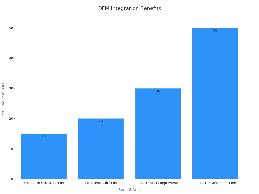
You can make a good prototype by following important dfm guidelines. These include putting parts in the best spots, keeping enough space, and making pads clear. Using dfm early can save 30% of design time. It also makes the product 15% better in electronics manufacturing.
Industry | Reduction in Design Time | Reduction in Production Costs | Improvement in Product Quality |
|---|---|---|---|
Electronics Manufacturing | 30% | 25% | 15% |
You can stop expensive delays by using dfm guidelines early. Working with LTPCBA helps your prototype process stay simple and fast.
Key Takeaways
Use important DFM rules like good part placement, enough space, and right pad design. This helps make your prototype easy and quick to build.
Add test points and clear labels. This helps you find problems early and stop expensive mistakes during assembly.
Work with LTPCBA for expert DFM checks and help. This saves time, lowers errors, and gets your prototype done right the first time.
Key DFM Guidelines
Component Placement
Smart component placement is very important for a good prototype. Put parts in an order that matches how the board is built. Group parts that are alike together. Make sure all parts face the same way. This helps machines work faster and makes fewer mistakes. Using special tools can help you make the best layout. This makes your board work better and last longer.
Keep sensitive parts away from things that get hot.
Put connectors near the edge so they are easy to reach.
Do not put tall parts next to small ones. This stops shadows when soldering.
Tip: LTPCBA’s SMT assembly experts use special software to check your layout. They give advice to help you follow dfm rules and make your assembly better.
Good placement of parts can make assembly faster. It also means less fixing and better board quality. This helps you finish your prototype quicker and with better results.
Good placement saves money by using less time and making fewer mistakes.
Keeping parts the same way makes machine setup faster.
Putting parts in the right place stops expensive fixes.
Spacing and Clearance
You need to follow dfm rules for spacing and clearance. This keeps your board safe and working well. Leave enough space between pads, traces, and parts. This stops short circuits and keeps the board from getting too hot.
Performance Metric / Guideline | Explanation |
|---|---|
Electrical Safety | Good spacing stops sparks between high voltage traces. This keeps the board safe and stops shorts. |
Signal Integrity | Enough space stops signals from mixing. This keeps signals clear and stops problems. |
Manufacturing Reliability | Spacing rules match what factories can do. This lowers the chance of mistakes that cause shorts. |
EMI/EMC Compliance | Good clearance stops unwanted signals. This keeps the board working right. |
Thermal Management | Enough space helps heat move away. This stops heat damage and shorts. |
Compliance with Standards | Following rules like IEC 60601-1 means you have enough space to stop sparks and shorts. |
Testing and Verification | High voltage tests check if your board has good insulation and spacing. This stops failures. |
Always check your design with IPC and UL standards. LTPCBA’s team looks at your files to make sure you follow dfm rules. This lowers the chance of mistakes and helps you finish your prototype faster.
Pad and Via Design
You make your board better by designing pads and vias the right way. Use normal pad sizes and shapes for strong solder joints. Do not use pads that are too small or too close. This stops solder from joining parts by mistake.
Use NSMD pads for most SMT parts.
Only use via-in-pad if you really need it for tight spaces.
Cover vias near pads so solder does not flow away.
Note: LTPCBA’s engineers check your pad and via design to make sure it can be made. They use AOI and other checks to find problems early. This helps you get a 99.5% pass rate in pcb assembly.
Following these dfm rules helps you make fewer mistakes and finish faster. You also save money and make your product better. Most cost savings in manufacturing come from good design choices now.

When you use key dfm rules, you see real results: 1. You use fewer parts, which saves money and time. 2. You use standard parts, which lowers costs and makes things better. 3. You make designs that are easy to change and use again. 4. You design boards that are easy to make and do not need special finishes. 5. You make assembly simple, which means less work and fewer mistakes.
These steps help you finish your prototype faster and with fewer problems. LTPCBA’s dfm experience makes your pcb assembly smooth and easy.
PCB DFM Guidelines
Material Choices
Picking the right materials makes your board strong. Good material choices are the base of pcb dfm guidelines. You must think about how the board handles heat, electricity, and force. Studies show copper trace width and copper weight change how hot the board gets. For example, wider traces and more copper help keep the board cooler. A 140 mil wide trace with 1 oz./sq. ft. copper carrying 3 A gets about 10°C hotter. A 40 mil wide trace with 0.5 oz./sq. ft. copper carrying 1 A can get 30°C hotter. Using copper planes or pours can help lower the heat even more. You need to follow IPC standards and what the manufacturer says for picking materials. It is also important to use materials that the manufacturer has and can work with.
Following pcb dfm guidelines for materials saves money and time. DFM analysis and smart material picks can save up to $170,000 each year. You will have fewer mistakes, faster builds, and better boards. Many companies use value engineering, buy in bulk, and get materials nearby to save money and meet dfm rules.
Stack-up Considerations
Planning the stack-up is a big part of pcb dfm guidelines. Putting signal layers between ground planes helps signals and makes the board work better. Studies show this setup cuts electromagnetic interference by 55%. Good stack-up planning stops 62% of reflection problems in boards with many layers. If you split ground planes, you can get signal problems and impedance mismatches. Multi-layer boards with ground planes next to signal layers make signals better by 40% in fast boards.
You should keep copper layers under important routes. This step stops 78% of EMI problems. In rigid-flex boards, ground planes act like shields and block interference. Tests show that overlapping ground planes and using ground vias make the board stronger and more stable. These stack-up choices help you meet dfm rules and make your prototype pcb work better.
You follow pcb dfm guidelines to keep pcb manufacturing easy. Picking the right stack-up and materials helps you avoid big mistakes and makes high-quality boards.
Solder Mask & Silkscreen
Solder Mask Clearance
You must watch solder mask clearance when you design a PCB. The solder mask keeps copper traces and pads safe from solder bridges. If the solder mask is rough, it can hold water. This can cause short circuits and other problems. Using new ways like inkjet printing makes the mask more exact. It also cuts down on waste and helps your assembly go faster.
Experts say you need at least 4 mil between pads for the solder dam. Green solder masks should have at least 4 mil clearance too. Do not cover big vias with solder mask because this can cause problems. Always make the solder mask a bit bigger around pads. This helps if things do not line up right during making. AOI and SPC tools check if the solder mask is in the right place. They help keep the board quality the same every time.
Tip: LTPCBA uses AOI and SPC to check the solder mask. This helps stop problems like solder bridges and pads getting covered.
Silkscreen Markings
Clear silkscreen markings help people build and check the board. Keep silkscreen text at least 4.5 mil from the insulation. It should also be 5 mil away from copper pads or traces. Make sure the text is at least 25 mil tall and lines are 4 mil wide. These rules stop silkscreen from covering places where solder goes.
Put polarity marks and names where you can see them.
Check that silkscreen does not cover pads or vias.
For crowded boards, use laser imaging for sharp marks.
Following IPC-A-600 Class 3 rules keeps silkscreen easy to read. LTPCBA checks your silkscreen to make sure it is clear and in the right spot. This helps your assembly go smoothly with fewer mistakes.
Design for Manufacturability
Test Points
Adding test points early makes your prototype more reliable. Test points help you check signals and see if the board works. They let engineers find problems fast and fix them before making lots of boards.
Test points help you watch and control how the board is made.
You can use them to see if your board is good quality.
They help you find mistakes and make testing faster.
Studies show test points on whole assemblies give better results. You can connect design, making, and quality data. This helps you guess part quality and get more good boards. Teams using test points finish work faster and have more success. You also make fewer mistakes and do not need to redo work.
Tip: Always add test points for power, ground, and important signals. LTPCBA’s dfm experts check your layout to see if you have enough test points for good testing.
Labeling & Polarity
Clear labels and polarity marks are very important for making boards. You help workers avoid mistakes by marking each part’s direction. Use silkscreen or laser marks to show pin 1, plus and minus sides, and part names.
Put labels where you can still see them after assembly.
Use common symbols and easy-to-read text for all marks.
Check that polarity marks match your drawing.
Good labels help dfm by making checking and testing easier. You stop confusion and make assembly go faster. LTPCBA checks your labels and polarity marks as part of their dfm review. This makes sure your prototype meets high standards and passes checks the first time.
Common Pitfalls
Orientation Errors
If you do not check part orientation, you can have big problems. Many prototype boards fail when parts like diodes, ICs, or LEDs are put in the wrong way. Machines use your design files to know how to place parts. If pin 1 or polarity is not marked clearly, mistakes can happen during assembly. These mistakes can make the board stop working or break parts. Always look at your silkscreen and layout to make sure orientation marks are clear. Use arrows, dots, or notches to show which way parts go. LTPCBA’s team checks your files to find these mistakes before making your board.
Tip: Make sure your schematic and layout match. This step helps you avoid one of the biggest dfm problems in SMT assembly.
Ignoring Manufacturer Specs
You can have trouble if you do not follow what your manufacturer says. Each PCB factory has its own rules for pad sizes, spacing, and materials. If you do not use these specs, you might get soldering problems, weak connections, or even a broken board. These dfm problems can slow your project and cost more money. Always look at the manufacturer’s rules before you finish your design. LTPCBA gives you clear guides and help so you can meet all the rules.
Check pad sizes and spacing with LTPCBA’s advice.
Use the right materials and stack-ups for the best results.
Ask questions early so you do not need to make expensive changes later.
By watching out for these common mistakes, you make your prototype assembly easier and more dependable.
Working with LTPCBA
DFM Checks & Reviews
When you work with LTPCBA, you get a full dfm check before assembly. The team looks at your PCB design files for problems that could slow things down or cause mistakes. You get help through each step so nothing is missed:
The team checks your design rules to make sure your board can be made right.
They look at where you put parts to help heat move and signals stay strong.
They check for signal problems like crosstalk or impedance issues.
They look at vias and how they are routed to stop assembly problems.
They check the board size and holes to make sure everything fits.
The team makes sure your materials and design follow factory rules.
You get a report with tips on how to make things better.
They do a last check to make sure all problems are fixed before building.
This careful way of working helps most boards pass the first test, with rates from 95% to 98%. You get fewer mistakes, less waste, and your board is ready on time. Most customers are happy, with scores over 80%. This shows LTPCBA’s dfm checks help you get good results.
Communication & Support
You always know what is happening when you pick LTPCBA. The company answers fast and gives you help any time, day or night. You get answers quickly, so you can fix problems early and not get delayed. Full turn-key service means you do not have to talk to many vendors. This can make things up to 60% faster and saves money.
Metric | LTPCBA Quick-Turn | Traditional Assembly |
|---|---|---|
On-Time Delivery | 95-98% | 85-95% |
Cycle Time | 1-5 days | 2-6 weeks |
Customer Return Rate | <1% | <0.5% |
Tip: If you talk to LTPCBA’s team early, you get expert dfm advice and reviews. This help lets you launch products faster and with fewer mistakes.
When you use the best steps and work with LTPCBA, your prototype gets done faster and better. A study from Norway found that clear and same information helps stop delays and makes things turn out well.
You can count on LTPCBA for help and advice. They make it easy to go from your design to a finished board.
FAQ
What is DFM in PCB assembly?
DFM stands for Design for Manufacturability. You use it to make your PCB design easy to build, which helps you avoid errors and delays.
How does LTPCBA help with DFM?
You get expert reviews from LTPCBA. The team checks your files, finds problems, and gives advice. This support helps you finish your prototype faster.
Why should you add test points to your PCB?
Test points let you check signals and power. You find problems early and fix them before making many boards. This step improves your board quality.
See Also
Top Guidelines For Superior Quality In SMT Assembly Processes
Common Techniques And Workflow Steps In SMT Assembly
Understanding SMT And DIP Assembly In PCBA Production
Effective Strategies To Improve SMT Line Efficiency In PCBA
Ways To Enhance SMT PCB Assembly For Higher Efficiency And Yield