How to Design and Optimize Mixed PCBA for Maximum Performance
You can achieve optimal mixed PCBA capabilities by effectively separating analog and digital circuits, carefully selecting the right components, and optimizing your PCB stackup. When working with mixed PCBA capabilities, common issues include thermal management, design complexity, and testing challenges. To ensure quality, use visual inspection, AOI, and functional testing for thorough validation. LTPCBA specializes in mixed PCBA capabilities, providing expert solutions and ensuring high-quality design for maximum performance.
Typical performance issues in mixed PCBA capabilities:
Thermal dissipation challenges
Design complexity
Manufacturing difficulties
Testing challenges
Component Type | Advantages | Disadvantages |
|---|---|---|
SMT | Smaller size, cheaper, suitable for dense layouts | Prone to detachment under stress |
THT | Superior mechanical strength, better heat dissipation | Larger footprint, higher manufacturing complexity |
Key Takeaways
Separate analog and digital circuits to enhance performance. Use distinct ground planes and shield sensitive traces to minimize interference.
Optimize your PCB stackup by selecting appropriate materials and layer arrangements. This helps control impedance and improves thermal management.
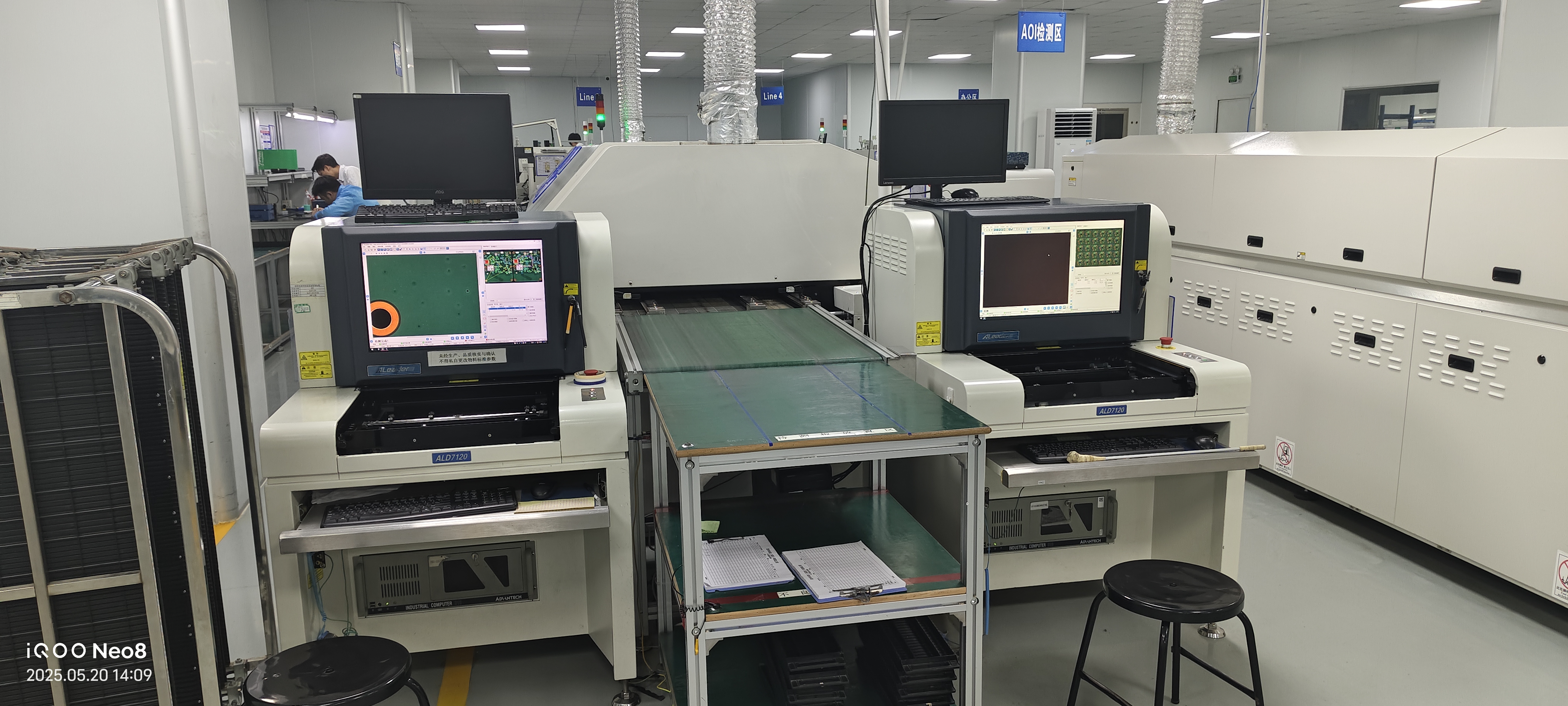
Implement thorough testing methods like visual inspection and automated optical inspection to ensure high-quality production and reduce defect rates.
Mixed PCBA Capabilities with LTPCBA
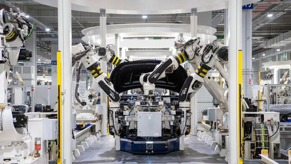
LTPCBA gives you a competitive edge in mixed pcba capabilities. You benefit from advanced automation, AI-driven defect prediction, and digital twins that optimize every step of the production process. You receive quality assurance through automated optical inspection, X-ray analysis, and functional testing. LTPCBA’s fast turnaround times—ranging from 1 to 5 days—help you accelerate your product launch.
Mixed Signal PCB Design Challenges
You face several challenges when working with mixed signal pcb. Noise interference between analog and digital circuits can distort signals. Grounding and power distribution issues may cause voltage fluctuations. Signal integrity and crosstalk threaten data reliability. Clock synchronization and timing jitter can result in glitches. Thermal management becomes critical as high-power components generate heat. Design for manufacturability and cost efficiency also require careful planning.
Analog and Digital Circuits Segregation
You must separate analog and digital circuits to achieve reliable mixed-signal pcb design. Place sensitive analog components in the analog plane and noisy digital components in the digital plane. Tie AGND and DGND pins to their respective ground planes. Use separate power supply blocks for analog and digital sections. Physical separation and shielding reduce interference. Grounding techniques like star grounding prevent noise propagation. These steps improve signal integrity and minimize noise in mixed pcba capabilities.
Optimizing Stackup and Materials
You optimize mixed pcba capabilities by selecting the right stackup and hybrid materials. A well-designed stackup confines electromagnetic fields, reduces emissions, and aids thermal dissipation. You can choose materials like standard FR4 for general electronics, high-Tg FR4 for industrial use, PTFE for high-speed data, and metal-core PCBs for power electronics. Proper spacing and clearances ensure efficient assembly and reliable soldering. Partitioning circuit areas and maintaining adequate clearances improve signal integrity and yield in mixed signal pcb.
Capability | Description |
|---|---|
Automation | Robotic systems manage material handling and inspection, minimizing human error. |
AI and Machine Learning | Predictive analytics help identify potential defects during etching or plating. |
Digital Twins | Virtual replicas of the production line optimize processes in real time. |
Eco-Friendly Practices | Use of lead-free finishes and recyclable materials aligns with global sustainability standards. |
Surface Mount Technology (SMT) | Enables high-density designs and faster production rates, with up to 100,000 components placed per hour. |
Through-Hole Assembly | Offers superior mechanical strength, ideal for environments prone to vibration. |
Mixed Technology | Combines SMT and through-hole components, ensuring effective solder mask alignment. |
Quality Control | Includes Automated Optical Inspection, X-Ray Inspection, In-Circuit Testing, and more to ensure reliability. |
High-Speed PCB Design and Performance Optimization
Signal Integrity and EMI Control
You must address signal integrity and EMI control as top priorities in high-speed mixed-signal pcb design. High-speed signals often introduce noise and crosstalk, which can degrade performance and reliability. You should maintain sufficient spacing between adjacent signal traces to minimize crosstalk. Place signal planes close to ground planes for shielding. Route traces perpendicular to each other to reduce interference. Series termination resistors help mitigate reflections, and short trace lengths prevent stubs and signal integrity problems.
Optimized pcb layout and routing minimize noise coupling. You should physically separate analog and digital components to prevent digital noise from affecting analog signals. Control clock and switching noise by routing clock traces on different layers from analog signals. Differential signaling for analog inputs rejects common-mode noise and enhances signal integrity.
Simulation tools allow you to predict circuit interactions and address potential signal integrity issues early in the design process. You can use these tools to model impedance control and optimize hybrid pcb stackup for high-performance pcbs.
You should ensure power and ground planes are in proximity to reduce PDN noise. Multiple low-inductance decoupling capacitors close to ICs filter noise. Match signal lengths using serpentine traces to minimize skew. These steps support optimization and reliability in mixed-signal pcb design.
Grounding, Shielding, and Power Distribution
Grounding and shielding play critical roles in mixed-signal pcb design. You should use a full ground plane for the best grounding solution. If space is limited, consider a grounding grid with as much area as possible to reduce impedance. Avoid bus wires, which create large loop inductances and receive high-frequency noise.
Proper component placement reduces crosstalk and enhances signal integrity by minimizing interference between analog and digital components. Shielding cans and enclosures prevent EMI from escaping and interfering with nearby devices. Controlled impedance traces ensure signals travel smoothly without significant loss or noise. Filter and decoupling capacitors maintain clean power delivery and minimize EMI. Optimize via placement and routing strategies to provide low-inductance paths for signals. Select low-loss pcb materials to maintain signal integrity at high frequencies. Control edges and apertures in shielding structures to minimize EMI leakage.
Challenge | Impact on Performance |
|---|---|
Can lead to overheating and power losses | |
Impedance mismatches | Results in voltage drops and inconsistent power delivery |
Ground bounce | Causes false switching and disrupts circuit operation |
Clean power delivery is crucial to avoid power ripples caused by switch-mode power supplies. Ground bounce from simultaneous digital signal switching can interrupt signals, leading to false switching. You must optimize power delivery and hybrid pcb stackup to meet design requirements for reliability and performance.
Manufacturability and Quality Assurance
Manufacturability and quality assurance are essential for efficient mixed-signal pcb production. You may encounter issues such as PCB layer alignment problems, via reliability challenges, delamination, blistering, and crosstalk. Advanced optical alignment systems during fabrication help prevent layer alignment issues. Sequential lamination processes and proper via filling improve via reliability. Controlled environments and optimized lamination parameters prevent delamination and blistering. Bake PCBs before assembly to remove trapped moisture.
Issue | Causes | Solutions |
|---|---|---|
PCB Layer Alignment Issues | Inaccurate drilling or imaging, thermal expansion, improper handling | Advanced optical alignment, material selection, strict quality control |
Via Reliability Problems | Poor plating, thermal stress, high aspect ratios | Sequential lamination, proper via filling, thermal cycling tests |
Delamination and Blistering | Moisture absorption, inadequate bonding, thermal mismatches | Controlled storage, optimized lamination, baking before assembly |
Crosstalk and EMI | Inadequate spacing, poor grounding, impedance mismatches | Increased trace spacing, guard traces, dedicated ground planes, simulation tools |
LTPCBA ensures quality assurance through advanced testing equipment such as X-ray, AOI, UV testing benches, and FCT equipment. An experienced procurement team sources quality materials from reputable distributors. The ERP system tracks materials and products, enhancing traceability and reducing errors. First article inspections minimize risks associated with incorrect or insufficient materials. Quality control tools analyze defects and implement preventive measures. A problem-solving team addresses existing defects and proposes comprehensive solutions. Quality personnel at each stage of production ensure reliability and optimization.
You benefit from measurable outcomes such as a 30% improvement in defect rates due to AI-driven AOI technology and a 99% defect-free PCB rate. High-definition cameras and advanced image analysis algorithms inspect PCBs for defects such as missing or misaligned components and solder quality.
Thermal management in mixed signal pcbs is crucial for reliability and performance. Overheating can lead to degradation and failure of electronic components. Effective temperature control lowers the risk of sudden shutdowns or malfunctions. Proper heat management increases component endurance and extends the system's lifespan. You should implement various thermal management techniques to ensure efficient operation under different thermal conditions. Optimization of hybrid pcb stackup, material selection, and layout supports long-term reliability.
Recent advancements in mixed-signal pcb design tools contribute to performance optimization. Star grounding stabilizes analog and digital sections. Filtering and decoupling ensure cleaner supply voltage. Noise-canceling circuits preserve signal quality in audio and wireless systems. High-frequency materials enhance signal integrity and minimize loss. AI and machine learning optimize circuit parameters dynamically, improving efficiency and adaptability in mixed-signal applications.
You must address design challenges, design requirements, and optimization strategies to achieve efficient mixed-signal pcb and high-speed pcb design. Focus on hybrid pcb stackup, material selection, impedance control, layout, and thermal management to ensure reliability and performance in mixed signal pcb and mixed-signal pcb design.
You achieve maximum mixed PCBA performance by grouping components by function, managing thermal distribution, and using proper grounding schemes.
Define board outline and constraints
Prioritize critical components
Conduct DRC/ERC checks
LTPCBA delivers unified quality, fast turnaround, and expert support for your projects.
FAQ
What is the best way to separate analog and digital circuits on a mixed PCBA?
You should place analog and digital sections on different areas of the board. Use separate ground planes and shield sensitive analog traces for optimal performance.
How do you minimize EMI in high-speed mixed-signal PCB designs?
Route high-speed signals over continuous ground planes.
Use short, direct traces.
Add decoupling capacitors near power pins.
Why is stackup selection important for mixed PCBA performance?
A well-chosen stackup controls impedance, reduces crosstalk, and improves thermal management. You ensure signal integrity and reliability by selecting the right materials and layer arrangement.
See Also
Essential Strategies for Enhancing SMT Line Efficiency
Techniques for Assembling Flex PCBs to Maximize Efficiency
Crucial Actions to Boost PCBA Reliability and Longevity
Ways to Enhance Your SMT PCB Assembly for Better Results
Combining SMT and DIP Techniques for Superior Mixed Technology PCBs