Common Defects in SMT Circuit Board Assembly and How to Prevent Them
SMT circuit board assembly faces common defects that can impact your production yield and product reliability. For example, a single pcb may have 500 parts and 1,500 solder terminations, creating 2,000 opportunities for solder issues.
Parameter | Value / Description |
|---|---|
Number of parts per board | 500 |
Number of solder terminations | 1500 |
Total defect opportunities | 2000 (sum of parts and terminations) |
Quality level | 6 Sigma (3.4 PPM defect rate per opportunity) |
SMT process yield (Y_SMT) | 99.32% (calculated as 0.9999966^2000) |
Defects per Unit (DPU) | 0.0068 (calculated as ABS(ln(0.9932))) |
Fault coverage at test stage | 50% (only half of detectable faults covered) |
Apparent test yield (Y_a) | 99.66% (calculated as e^(-DPU × fault coverage)) |
Required fault coverage for 100 PPM quality | 99.5% (to achieve 100 PPM quality level at test stage for this 6-Sigma process) |

You can prevent most smt defects by understanding the root causes, such as solder paste printing errors, which account for up to 90% of soldering faults in smt pcb assembly. LTPCBA uses advanced surface mount technologies and process solutions to ensure high-quality pcb assembly and reliable soldering results.
Key Takeaways
Most SMT defects come from solder paste printing errors, so controlling this step improves yield and reduces rework.
Common defects like solder bridges, tombstoning, cold joints, and misalignment can be prevented by optimizing stencil design, reflow profiles, and equipment calibration.
Using advanced inspection methods like AOI and X-ray, combined with strong process monitoring, helps catch defects early and ensures reliable PCB assembly.
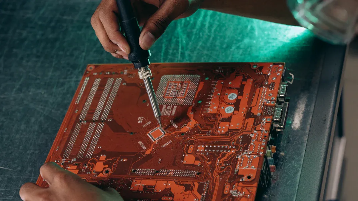
Common Defects in SMT PCB Assembly
Surface mount technology brings speed and efficiency to pcb assembly, but it also introduces specific challenges. You need to recognize and address these common defects early to maintain high quality and reliability in your smt circuit board assembly. The following sections break down the most frequent issues, their causes, and practical solutions.
Tip: Over 60% of quality defects in smt pcb assembly originate from solder paste printing. Early detection and process control are essential for reducing costly rework and improving first pass yield.
Solder Bridges
Solder bridges occur when excess solder forms an unintended connection between two or more adjacent pads or leads, causing short circuits. This defect often results from too much solder paste, improper stencil design, or misaligned printing.
Why it happens:
Narrow clearance between pads
Poor stencil design or misalignment
Incorrect reflow profile
How to prevent it:
Use optimized stencil thickness and aperture size.
Maintain precise alignment during solder paste printing.
Follow strict solder mask design rules to ensure proper pad spacing.
Control reflow soldering parameters, such as peak temperature and time above liquidus.
Regularly inspect with AOI and SPI systems.
LTPCBA uses advanced stencil designs, automated solder paste inspection, and real-time process monitoring to minimize solder bridges. By controlling these variables, you can significantly reduce this common defect in smt circuit board assembly.
Tombstoning
Tombstoning, also known as the tombstone effect, happens when one end of a chip component lifts off the pad during reflow, resembling a tombstone. This defect disrupts electrical connections and can cause intermittent faults.
Why it happens:
Uneven wetting forces during reflow soldering
Incorrect reflow profile (temperature ramp or soak zone)
Imbalanced solder volume on pads
Poor thermal contact or pad design
How to prevent it:
Adjust the soak zone temperature upward by a few degrees to balance wetting.
Reduce the ramp rate during preheat to minimize the tombstoning effect.
Ensure accurate thermocouple placement for reliable thermal profiling.
Use rolling-average filters to smooth thermal data and avoid profile errors.
Optimize pad design and solder paste volume.
LTPCBA’s process engineers fine-tune reflow profiles and use precise thermal monitoring to reduce tombstone defects. These solutions help you control the causes of tombstoning and improve assembly quality.
Cold Joints
Cold joints are weak or unreliable solder connections that appear dull or grainy. They often result in poor electrical contact and can lead to intermittent failures.
Why it happens:
Insufficient heat during soldering
Contaminated surfaces or oxidation
Inadequate solder alloy or flux activity
Improper reflow soldering profile
How to prevent it:
Use oxygen-free environments or vacuum soldering to reduce voids.
Select appropriate solder alloys for your application.
Maintain clean surfaces and proper flux application.
Monitor and control reflow soldering parameters, including temperature and dwell time.
LTPCBA leverages vacuum reflow and advanced process controls to eliminate cold joints, ensuring strong and reliable solder joints in every pcb assembly.
Misalignment
Component misalignment occurs when parts are not placed accurately on their pads, leading to poor soldering and potential functional failures. This is one of the most common pcb assembly faults.
Why it happens:
Inaccurate pick-and-place machine calibration
Solder paste misprinting
PCB warping during reflow
Excessive vibration or movement during assembly
How to prevent it:
Calibrate placement equipment regularly.
Use high-precision pick-and-place machines and vision alignment systems.
Implement AOI for real-time detection and correction.
Optimize reflow profiles to prevent component movement.
Train operators thoroughly and use digital twins for predictive maintenance.
LTPCBA employs Industry 4.0 technologies, including AI-driven placement and AOI, to ensure precise component alignment and high assembly quality.
Solder Balls
Solder balls are small, round particles of solder that form near joints or under components during reflow. They can cause short circuits, electrical leakage, and reduce pcb reliability.
Why it happens:
Improper solder paste printing or excessive paste
Moisture in solder paste or pcb
Incorrect reflow profile (ramp-up or cooling rate)
Contaminated surfaces or poor flux activity
How to prevent it:
Maintain reflow ramp-up rates below 3°C/s and cooling rates below 4°C/s.
Use SPI to monitor solder paste thickness and coverage.
Store solder paste and pcbs in controlled environments to prevent moisture absorption.
Clean equipment regularly and use high-quality solder paste.
Follow IPC acceptability criteria for solder ball size and spacing.
LTPCBA’s process audits, AOI, and statistical process control help you detect and eliminate solder balls, supporting high first pass yield and low defect rates.
Missing Components
Missing components are parts that fail to be placed or soldered onto the pcb during assembly. This defect can cause immediate product failure or latent faults.
Why it happens:
Pick-and-place machine errors or misfeeds
Blocked or insufficient solder paste on pads
Excessive placement pressure
Miniaturization increasing placement difficulty
How to prevent it:
Use AOI and SPI at multiple stages to detect missing parts early.
Apply statistical process control to monitor placement accuracy.
Train operators in equipment handling and defect identification.
Verify BOM and component footprints during DFA review.
LTPCBA’s automated inspection systems and operator training programs ensure missing components are caught and corrected before final assembly.
Non-Wetting
Non-wetting occurs when solder fails to bond properly to the pad or component lead, resulting in weak or open connections.
Why it happens:
Contaminated or oxidized surfaces
Insufficient heat during reflow soldering
Inadequate flux activity
Poor solder paste quality
How to prevent it:
Monitor oven temperature zones and conveyor speeds for consistent thermal performance.
Use AOI after reflow to detect non-wetting defects.
Apply SPC to track solder paste volume and placement accuracy.
Conduct regular process audits and root cause analysis.
LTPCBA’s quality assurance team uses real-time data and process audits to identify trends and implement corrective solutions for non-wetting, ensuring robust solder joints.
Warped Components
Warped components or pcbs bend or twist during assembly, leading to poor soldering and mechanical stress.
Why it happens:
Uneven heating or cooling during reflow
PCB design with inadequate support or infill line direction
High thermal gradients and residual stress
How to prevent it:
Use predictive modeling and simulation to optimize thermal profiles.
Design pcbs with proper support and infill direction.
Control reflow oven settings to minimize thermal gradients.
Verify warping trends with experimental and simulation data.
LTPCBA applies finite element analysis and real-time thermal monitoring to predict and prevent warping, maintaining assembly quality and reliability.
Common PCB Assembly Faults
Common pcb assembly faults include thermal management issues, contamination, documentation errors, and equipment calibration problems. These faults can impact product appearance, electrical reliability, and overall assembly quality.
How to prevent them:
Design proper thermal relief patterns and use simulation tools.
Maintain clean room conditions and proper handling procedures.
Implement digital documentation and regular process audits.
Schedule preventive maintenance and calibration for all equipment.
Use advanced inspection techniques like AOI, X-ray, and in-circuit testing.
Train employees continuously and foster a culture of quality improvement.
Note: LTPCBA’s comprehensive quality management system, including AOI, X-ray inspection, and adherence to international standards, ensures that you receive reliable solutions to defects in chip mounting and all stages of smt circuit board assembly.
By understanding these common defects and applying targeted solutions, you can achieve high-quality, reliable pcb assembly. LTPCBA’s expertise and commitment to quality help you minimize defects in chip mounting and maintain industry-leading standards in smt circuit board assembly.
Process Control and Inspection in SMT Circuit Board Assembly
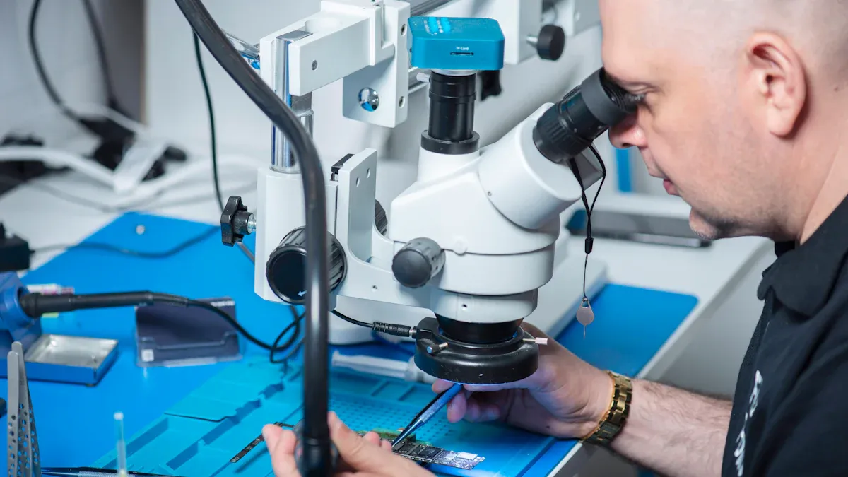
Effective process control and inspection are essential for high-quality smt circuit board assembly. You need to apply strong process control measures in reflow soldering and use advanced inspection systems to catch defects early. These solutions help you maintain reliable pcb production and reduce costly rework.
DFM and DFA Principles
Design for Manufacturability (DFM) and Design for Assembly (DFA) guide you to create pcb layouts that simplify smt assembly. When you follow DFM and DFA, you reduce the risk of soldering defects and improve solder joint reliability. You should check pad sizes, component spacing, and solder mask design before starting assembly. These steps help you avoid common solder issues and make reflow soldering more consistent.
AOI and X-ray Inspection
Automated Optical Inspection (AOI) and X-ray systems play a key role in smt circuit board assembly. AOI checks for missing parts, solder bridges, and misalignment on the pcb surface. X-ray inspection finds hidden solder defects, such as voids and cracks under BGA packages, that AOI cannot see. The table below compares their effectiveness:
Metric | AOI | X-ray Inspection |
|---|---|---|
Defect Detection Accuracy | 95-99% (surface defects) | |
Inspection Speed | 1000+ boards/hour | Slower, more detailed |
Cost | Lower | Higher |
You benefit from both AOI and X-ray, as they improve first-pass yield and reduce rework by catching soldering problems at every stage.
Process Monitoring
You should use process monitoring tools like Statistical Process Control (SPC) and Six Sigma to track solder paste printing, placement, and reflow soldering. AOI and SPI systems provide real-time data on solder volume, pad coverage, and solder joint quality. Control charts and root cause analysis help you spot trends and fix soldering issues before they affect the whole assembly. Layered inspection—SPI, AOI, X-ray, and manual checks—ensures you catch defects early and keep your smt assembly process stable.
LTPCBA Quality Assurance
LTPCBA uses advanced pick-and-place machines, AOI, and X-ray inspection to deliver high-quality smt circuit board assembly. The company follows strict standards like IPC-A-610 and ISO 9001 for pcb quality control. Automated inspection reduces error rates and speeds up production. LTPCBA achieves a 99.95% placement success rate and a 95% first-pass yield. You can trust LTPCBA for reliable solutions and consistent quality in every pcb assembly.
You improve SMT circuit board assembly quality by using strong process control and early defect prevention. The table below shows how these steps boost results:
Metric | Change Observed |
|---|---|
Defect escape rate | |
First-pass yield | Increased to 98% |
When you choose LTPCBA, you gain faster design, fewer errors, and reliable PCBs across many industries.
FAQ
What is the most common defect in SMT PCB assembly?
You often see solder bridges as the most common defect. Solder paste printing errors usually cause this issue. Careful process control helps you prevent it.
How does LTPCBA ensure high-quality SMT circuit board assembly?
You benefit from LTPCBA’s automated inspection, strict process monitoring, and adherence to international standards. These steps help you receive reliable and consistent PCB assemblies.
Can you reduce defects by using AOI and X-ray inspection?
Yes, you can.
AOI finds surface defects quickly.
X-ray inspection detects hidden faults under components.
Both methods improve your assembly quality.
See Also
Typical Reflow Soldering Flaws In SMT And How To Prevent
Key Technical Concerns For VIPPO PCBs During SMT Assembly
Reasons Components Detach During Wave Soldering In SMT Production
Effective Methods To Clean PCB Boards After SMT Assembly
Important Considerations For SMT Assembly Of Rigid-Flex PCBs