How to Avoid Common Pitfalls in PCBA Prototype Assembly
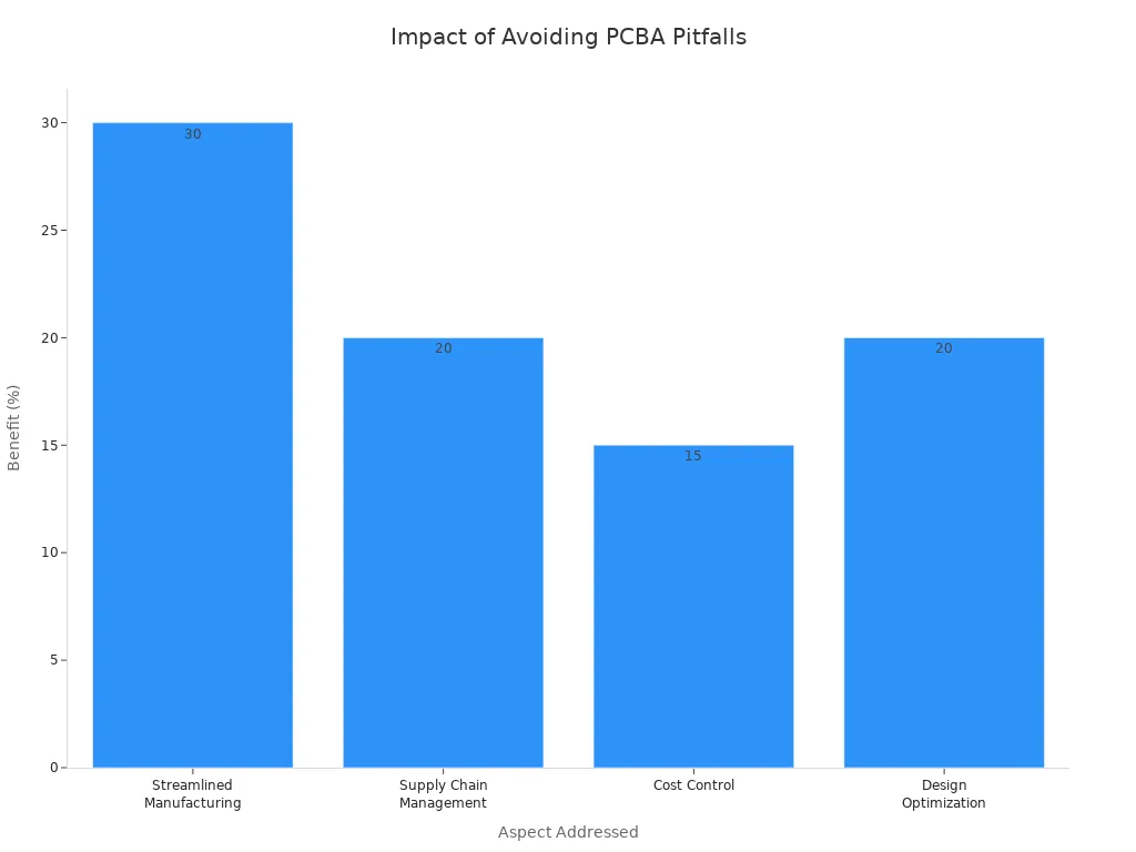
You can avoid costly setbacks in pcba prototype assembly by focusing on design optimization, clear documentation, and thorough testing. By streamlining your pcba prototype assembly process and choosing standard components, you can reduce production costs by over 20%. Implementing rigorous design-for-manufacturability steps in your pcba prototype assembly also increases manufacturing yield by 15%. These enhancements result in faster product launches and fewer supply chain issues, making your pcba prototype assembly project more reliable and cost-effective.
Key Takeaways
Double-check your design early using design rule checks and peer reviews to catch errors before assembly.
Source reliable components and plan for lead times to avoid delays and quality issues in your prototype.
Follow design for manufacturability (DFM) principles to reduce defects, lower costs, and speed up production.
Communicate clearly and collaborate early with your assembly provider to ensure smooth project execution.
Use automated inspection methods like AOI and thorough testing to find defects early and improve product quality.
Common Pitfalls
Design Errors
Design errors often cause the most trouble in pcba prototype assembly. You can avoid many problems by understanding the most frequent mistakes and their effects. The table below highlights common design errors and their impacts:
Common Design Error | Description and Impact |
|---|---|
Incorrect laying patterns | Poor pad spacing makes soldering difficult and increases the risk of defects. |
Narrow high-current traces | Thin traces overheat and may fail, especially on inner layers with less heat escape. |
Use of blind or hidden vias | These vias complicate the design and can disrupt board function. |
Lengthy high-speed traces | Long or winding traces reduce signal quality and slow down microprocessors. |
Wrong placement of decoupling capacitors | Bad placement causes unstable voltage and more noise, harming device operation. |
Incorrect antenna placement in wireless | Poor layout lowers power transfer and wireless performance. |
Improper testing and lack of review | Skipping tests lets small errors go unnoticed, risking board failure. |
Tip: Always double-check your design with a peer or use design rule checks before moving to pcb assembly. Early detection of errors saves time and money.
Design errors can lead to misaligned components, unrouted signals, and power issues. For example, if you place a component incorrectly, you might create a short circuit or an open connection. Routing mistakes can cause signal problems and device failures. Poor power layout may result in overheating and unstable voltage. If you do not manage thermal reliefs well, you risk cold solder joints and warped boards. These issues lower your assembly yield and increase costs. You can prevent most of them by using design verification tools and following industry standards.
Component Issues
Component problems are another major source of failure in pcb assembly. You face risks from both the parts themselves and how you handle them. Here are the most common types of component issues:
Mechanical failures: Parts can bend, crack, or break due to stress or fatigue.
Environmental failures: Moisture, dust, vibration, and heat can damage sensitive components.
Electrical stress failures: Electrostatic discharge, overvoltage, and dielectric breakdown can destroy parts.
Packaging failures: Corrosion, thermal expansion, and cracked wire bonds often lead to malfunction.
Aging failures: Old or worn-out parts may fail before your product reaches the market.
Solderability issues: Oxidized leads or poor solder mask design cause weak joints.
You can reduce these risks by sourcing components from reliable suppliers and checking for damage or authenticity when parts arrive. Always plan for lead times and possible shortages. If you use obsolete or hard-to-find parts, you may face delays or need to redesign your board. Kitting services and turnkey pcb assembly providers can help you manage inventory and avoid missing or incorrect parts. Regular supplier audits and incoming inspections also help maintain quality.
Assembly Mistakes
Assembly mistakes can quickly ruin even the best-designed pcb assembly. These errors lower your yield and force you to spend extra time on rework. The table below shows common assembly mistakes, their impacts, and how you can avoid them:
Assembly Mistake | Impact on Yield and Rework Rates | Recommendations to Mitigate Impact |
|---|---|---|
Pad-to-Solder Ratio Misjudgment | Weak solder joints, hidden failures, more rework, unhappy customers | Use IPC-compliant pad-to-paste ratios and set soldering profiles |
Material Traceability Gaps | Hard-to-find defects, batch recalls, more rework | Track batches with IDs and use MES for traceability |
Pick-and-Place Path Interference | Misaligned parts, shorts, weak joints, more defects | Calibrate machines and use optical checks for critical components |
Soldering Atmosphere Instability | Voids, poor joints, shorter component life, lower reliability, more rework | Monitor nitrogen levels and test solder paste in different settings |
Final Inspection Blind Spots | Missed defects, failures after shipping, lost customer trust | Use X-ray for hidden parts and design tests for reliability |
Note: Automated inspections and functional tests during pcb assembly catch most mistakes early. Training your team and using advanced equipment also help reduce errors.
Common assembly errors like solder bridges, tombstoning, and misalignment increase the number of defective boards. These problems force you to rework or scrap boards, raising costs and delaying your project. You can improve your yield by following strict quality control steps, using automated inspection, and standardizing your assembly process.
Design for Manufacturability
DFM in pcba prototype assembly
You can improve your pcb assembly process by following key design for manufacturability (DFM) principles. These steps help you avoid costly mistakes and make your project more reliable. When you focus on design for assembly, you make it easier for manufacturers to build your board without errors. Here are some important DFM practices you should use:
Start early by working with your manufacturer. Early collaboration helps you match your design to real manufacturing capabilities.
Run DFM checks at every stage. This lets you catch problems before they become expensive to fix.
Group similar components together and keep their orientation consistent. This makes the pcb assembly process smoother and reduces placement errors.
Use best practices for trace routing. Try to use 45-degree angles and keep trace widths consistent.
Design vias carefully. Avoid placing vias in surface mount pads and choose the right via type for your needs.
Balance your layer stack-up. Think about impedance control and the materials you use.
Follow clear solder mask and silkscreen guidelines. Good markings and clearances help during assembly and inspection.
Use DFM analysis tools. These tools find manufacturability issues that you might miss.
When you apply these design for assembly steps, you reduce defects, lower costs, and speed up your time to market. You also improve the reliability of your pcba prototype assembly.
Tip: Always document your DFM checks and share them with your manufacturer. This helps everyone stay on the same page.
Using Design Rule Checks
Design rule checks (DRC) play a big role in the pcb assembly process. You use DRC tools to make sure your design meets all the rules for spacing, size, and placement. These checks help you find errors like missing pins, shorts, or clearance problems before you build the board.
DRC tools check electrical, physical, and manufacturing rules.
They catch issues with component placement, orientation, and spacing.
You can also use DRC for design for assembly and design for testing.
A well-run DRC process leads to fewer board re-spins, better yield, and lower costs. You also meet industry standards and improve your board’s performance. When you combine DRC with design for assembly, you create a strong foundation for a successful pcb assembly process.
DFM Practice | Benefit |
|---|---|
Early collaboration | Fewer design changes, faster builds |
Proper spacing and layout | Fewer soldering errors, easier repairs |
Clear markings | Less confusion, faster assembly |
Good thermal management | Longer component life, fewer failures |
Component Placement
Spacing & Orientation
You improve your PCBA prototype assembly by following smart spacing and orientation rules. Proper spacing keeps your components safe and makes assembly easier. You should:
Keep at least 125 mils between the board edge and SMD components. This prevents damage during depanelization.
Space copper traces at least 10 mils from the board edge. This allows for a solder mask gap and avoids pad encroachment.
Maintain a minimum drill-to-copper distance of 8 mils and annular ring to pad edge spacing of 7 mils.
Group similar components together and align them with the same orientation. For example, place all QFPs in a row with pin 1 at the same corner.
Avoid placing components too close to the board edge. This reduces the risk of damage during automated assembly.
Use correct SMT pad sizes to prevent tombstoning and solder bridging.
Orient discrete components so pins enter wave solder at the same time. Place larger parts after smaller ones to avoid shadowing.
Follow IPC standards such as IPC-A-600 and IPC/WHMA-A-620C for quality and acceptance.
Tip: Grouping components with similar functions improves assembly efficiency. Standardized orientation makes identification and placement easier, reducing errors and saving time.
Leaving enough space around each part allows easier access during placement and soldering. Consistent orientation helps technicians work faster and with fewer mistakes. Good spacing also minimizes issues like solder bridging and tombstoning. You boost reliability and reduce costs by following these guidelines.
Large & High-Speed Parts
Placing large and high-speed components brings unique challenges. Large connectors and capacitors need strong physical connections and secure mounting. You should use through-hole technology for these parts because it provides better mechanical strength than surface-mount technology.
Position large components with enough clearance to avoid interference with mounting brackets or housings.
Define form factor and physical requirements early in the design phase. This helps you avoid layout problems and costly redesigns.
Use robust inspection and testing protocols. Functional and environmental testing ensures your board works under real-world conditions.
Place heat-sensitive components away from high-temperature parts to improve thermal management.
Ensure test access points for effective prototype testing.
High-speed parts require careful layout to maintain signal integrity. You should avoid placing these components too close together. Adopting Design for Manufacturability (DFM) principles helps you prevent signal issues and manufacturability concerns.
Note: Partnering with experienced suppliers and contract manufacturers helps you match technology to manufacturing facilities. This maximizes yield and minimizes cost.
Strong supply chain management and quality systems support reliable assembly. Prototyping lets you catch problems early, reducing delays and improving your final product.
Documentation
Essential Files
You need to prepare a complete set of files before starting your PCBA prototype assembly. These files help you communicate your design clearly and avoid mistakes during manufacturing. The most important files include:
Gerber files: These files show the copper layers, solder mask, and silkscreen. Manufacturers use them to create your PCB.
Bill of Materials (BOM): This list includes every part you need, with part numbers, values, and footprints. Accurate BOMs prevent sourcing delays and wrong parts.
Centroid data (Pick-and-Place files): These files tell the assembly machines where to place each component.
Assembly drawings: These drawings show the exact location and orientation of each part.
Test point files: These files mark where you or your manufacturer can test the board after assembly.
Tip: Double-check your BOM for correct part numbers and footprints. Mistakes here often lead to rework or delays.
A complete documentation package ensures your manufacturer understands your requirements. You reduce the risk of errors, such as misplaced components or missing parts, by providing all essential files.
Detailed Drawings
Detailed drawings play a key role in reducing errors during PCBA prototype assembly. You should include clear assembly drawings, notes, and callouts in your documentation. These drawings help your manufacturer see exactly how your board should look.
Follow Design for Manufacturability (DFM) guidelines to keep proper clearances and avoid layout problems.
Verify BOM accuracy to ensure correct parts and footprints.
Collaborate with your manufacturer early to solve manufacturability concerns.
Add test points to make debugging easier and reduce rework time.
Experts agree that detailed assembly drawings, combined with Gerber files, BOM, and centroid data, provide clear instructions for your project. This clarity helps prevent errors like incorrect footprints or misplaced parts. Including notes in your BOM and drawings also helps avoid sourcing delays and manufacturing mistakes. In one case, early DFM checks with detailed drawings caught an oversized footprint, saving time and money.
When you invest time in creating detailed documentation, you set your project up for success. You help your manufacturer deliver a board that matches your design and works as expected.
Communication with LTPCBA
Early Collaboration
You set your project up for success when you start working with LTPCBA early in the process. Early collaboration with a reliable pcb assembly service brings many advantages:
You and your LTPCBA team can hold daily meetings and share progress reports. This keeps everyone aligned and helps catch issues before they grow.
Stand-up meetings and peer reviews help you spot design flaws and resolve them quickly.
You benefit from integrated processes that save costs and speed up your time-to-market.
LTPCBA uses advanced inspection tools like AOI and X-ray to ensure high quality from the start.
You can scale your project easily, moving from prototypes to larger production runs without delays.
LTPCBA’s certifications, such as ISO 9001 and IPC-A-610, guarantee strict quality control.
When you work closely with LTPCBA, you detect design issues early, such as thermal management or testability problems. This reduces the need for expensive corrections later. You also gain access to reliable component sourcing and advanced testing, which keeps your pcb assembly project on track.
Tip: Early collaboration with your pcba service provider lets you focus on innovation while experts handle the assembly details.
Sharing Requirements
Clear communication of your requirements is key to a smooth pcb assembly process. You should always share detailed assembly drawings, a complete Bill of Materials (BOM), and your project timeline with LTPCBA. This prevents misunderstandings and sets clear expectations.
Share your BOM with alternatives to avoid sourcing delays.
Provide assembly drawings and test procedures to help LTPCBA plan production and quality checks.
Communicate your quality standards and regulatory needs from the start.
When you give LTPCBA accurate product dimensions and prototypes, you help them assess production feasibility and avoid fit issues.
Early Design for Manufacturability (DFM) discussions with LTPCBA optimize component placement and testing.
Sharing detailed requirements allows LTPCBA to offer design insights and ensure your board meets all standards.
This approach leads to faster project timelines, fewer errors, and higher product quality.
You build a strong partnership with LTPCBA by sharing your needs clearly. This results in smoother project execution and reliable pcb assembly service every time.
Testing & Inspection
AOI & Quality Checks
You need strong inspection methods to catch defects early in your PCBA prototype assembly. Automated Optical Inspection (AOI) uses high-resolution cameras to scan your boards and compare them to a perfect sample. AOI finds missing parts, misaligned components, and soldering problems much faster than manual checks. In fact, AOI inspects PCBs over 80 times faster than the human eye and detects about 25% more defects. When you use 3D AOI, you can spot even more issues, such as lifted leads or low solder volume, which are hard to see in 2D images.
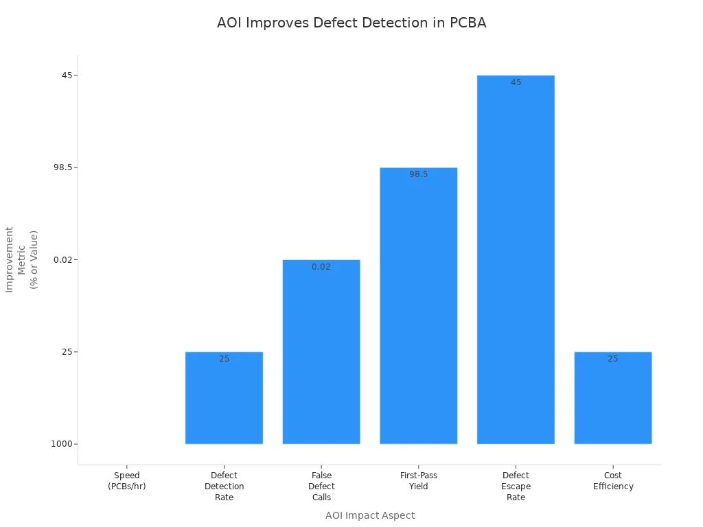
AOI also reduces false alarms and boosts your first-pass yield to nearly 98.5%. Early inspection with AOI can cut rework costs by up to ten times. You can use AOI before and after soldering to catch problems right away. This keeps your assembly process smooth and saves time and money.
You can combine AOI with other inspection methods for even better results. Here is a quick comparison of common testing methods:
Testing Method | Key Features | Best Use Case |
|---|---|---|
AOI | Fast, automated, high accuracy; detects visual defects and solder issues | All stages, especially prototypes and small runs |
Flying Probe Test | No custom fixtures; robotic probes test points; flexible for design changes | Early-stage debugging, small batches |
Manual Visual Inspection | Simple, low-cost; relies on human eye | Basic checks, simple boards |
In-Circuit Testing | Bed-of-nails fixture; tests each component electrically | Mass production |
Tip: Use AOI and flying probe tests together for the best mix of speed, flexibility, and defect coverage in your prototypes.
Functional Testing
Functional testing checks if your assembled board works as intended in real-world conditions. You run your PCBA through typical tasks, making sure every part performs its job. This step finds problems that visual checks might miss, such as logic errors or faulty connections.
Functional testing simulates how your product will be used.
It helps you catch software or hardware bugs before they reach customers.
You can use it to check interfaces, performance, and user experience.
Early fault detection here means less rework and fewer warranty claims.
Industries like aerospace rely on thorough functional testing to meet strict safety and reliability standards.
Thorough functional testing gives you confidence in your prototype. You know your board will perform well, even in tough environments. This step is essential for quality assurance and long-term reliability.
Sourcing Components
Long Lead Times
You may face long lead times when sourcing components for your PCBA prototype assembly. These delays often happen because of component shortages, allocation issues, and supplier coordination problems. Sometimes, demand for certain parts exceeds what manufacturers can produce. This causes uncertain lead times and can delay your project. If you use obsolete or end-of-life components, you might need to redesign your board or wait for replacements. Designers sometimes forget to check if parts are available before finalizing the design, which leads to sourcing difficulties later.
Other factors also add to the wait. Minimum order quantity requirements may not match your needs, so you either overbuy or wait longer. Logistics and customs can slow down shipments, especially if you source parts from overseas. Complex supplier coordination makes it harder to keep everything on schedule. Geopolitical events can disrupt supply routes and cause unpredictable delays.
Here is a summary of the main causes and their impact:
Cause | Description | Impact on Lead Time |
|---|---|---|
Component stockouts and long lead times | Parts go out of stock or have long waits, forcing redesigns or delays. | Directly increases sourcing time and delays assembly. |
Part obsolescence | Components become obsolete after a few years. | Leads to redesigns or sourcing delays. |
Mismatch between component and product lifecycle | Short component lifecycles complicate maintenance. | Causes long-term sourcing challenges. |
Lack of real-time supplier data | No up-to-date inventory or supplier info. | Increases uncertainty and procurement lead times. |
Geopolitical disruptions | Political events interrupt supply routes. | Causes unpredictable delays. |
MOQ constraints | Supplier minimums do not fit your needs. | Can delay procurement or increase costs. |
Complex supplier coordination | Managing many suppliers complicates schedules. | Leads to coordination delays. |
Logistics and customs delays | Shipping and customs issues stall timelines. | Adds unpredictable delays to component arrival. |
You can shorten lead times by working with suppliers early and checking part availability during design. Companies that use design for manufacturability and engage suppliers early have reduced lead times by up to 35%.
Standard vs. Custom Parts
Choosing between standard and custom parts affects your assembly timeline and risk. Standard parts are easier to find and usually cost less. You can source them quickly, and they rarely go obsolete. Custom or niche parts, on the other hand, often have longer lead times and higher risks.
Standard parts, like common resistor sizes, are widely available and have multiple suppliers.
You can include alternate standard components in your BOM to avoid delays if one part is out of stock.
Standard parts are less likely to become obsolete, so you reduce the risk of redesigns.
Custom parts may require special orders, which can take days or even weeks to arrive.
Using custom or niche parts increases the chance of supply chain problems, especially if only one supplier exists.
Turnkey manufacturers can often source standard parts within hours, but custom parts may take much longer.
Tools like Octopart or SiliconExpert help you check stock levels and lifecycle status, making it easier to choose standard parts.
You should validate your BOM after design verification but before ordering. This step lets you substitute unavailable parts and avoid last-minute surprises. Working with experienced suppliers and using real-time data tools helps you manage risks and keep your project on track.
PCB Assembly Guidelines
Following Manufacturer Specs
You achieve better results in pcb assembly when you follow manufacturer specifications closely. These guidelines help you avoid common mistakes and improve the reliability of your boards. Manufacturers recommend several key practices for every pcb assembly process:
Guideline Category | Key Recommendations | Why It Matters |
|---|---|---|
Use ISO 9001, IPC-A-610, and other industry certifications. | These standards ensure consistent quality and best practices. | |
Manufacturing Capabilities and Technology | Choose facilities with modern equipment and support for SMT, through-hole, and mixed technologies. | Advanced technology reduces defects and supports complex designs. |
Supply Chain Management and Component Sourcing | Work with reputable suppliers and maintain traceability for all components. | Good sourcing prevents counterfeit parts and improves reliability. |
Testing and Inspection Procedures | Use AOI, X-ray, ICT, and functional testing with trained staff. | Rigorous testing finds defects early and improves product quality. |
Communication and Customer Support | Keep open communication and provide regular updates. | Clear communication helps resolve issues quickly and keeps projects on track. |
You should also use visual inspection, in-circuit testing, and X-ray inspection during the pcb assembly process. These steps help you catch solder joint defects, incorrect component placement, and shifting during soldering. Following these guidelines leads to fewer errors and higher first-pass yields.
LTPCBA Best Practices
LTPCBA sets a high standard for pcb assembly by using advanced technology and strict quality control. You benefit from their 100% automated optical inspection and X-ray testing, which keep defect rates below 0.05%. LTPCBA uses modern SMT placement machines that handle complex pcb assembly projects with precision.
Dedicated project managers give you daily updates and respond quickly to design changes.
Strong supply chain partnerships help LTPCBA deliver prototypes on time, even during global disruptions.
LTPCBA protects your intellectual property with NDAs and secure data handling.
You can request case studies and references to see proven results.
The table below shows how LTPCBA’s quality control improves outcomes:
Quality Metric | Before LTPCBA QC | After LTPCBA QC | Improvement |
|---|---|---|---|
Defect Rate | 0.91% | 0.14% | Reduced by 0.77% |
Defects Observed | 366 | 58 | Decreased by 308 |
Lot Reject Rate (PPM) | 5500 | 900 | Reduced by 4600 PPM |
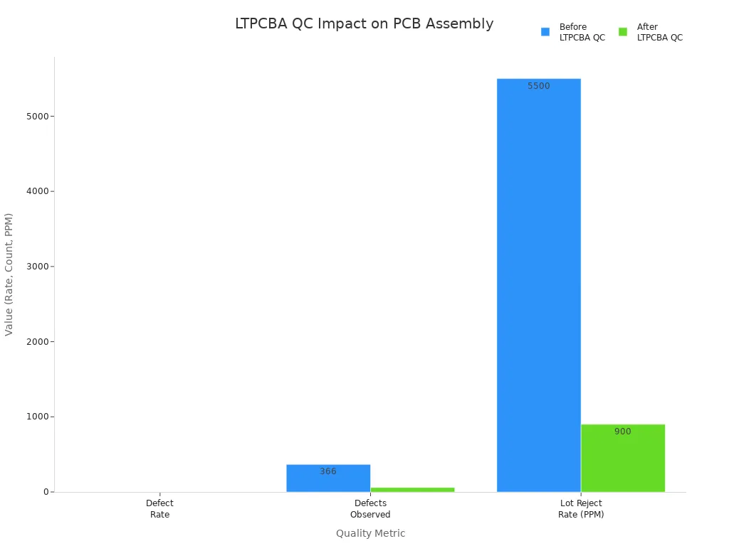
LTPCBA’s best practices include a first pass yield of 95%, pick-and-place accuracy of 99.95%, and a pass rate of 99.5%. These numbers show that you can trust LTPCBA for reliable pcb assembly. Their quick-turn services also help you get prototypes in as little as 24–48 hours, supporting fast development cycles.
Tip: When you follow manufacturer specs and use LTPCBA’s expertise, you reduce errors, save time, and improve the success of your pcb assembly projects.
Circuit Board Assembly Tips
Material & Thermal Choices
You make better decisions in circuit board assembly when you understand how materials and thermal management affect your project. The right substrate materials help your board handle heat and last longer. Here are some important points to consider:
Choose PCB substrates with high glass transition temperature (Tg) and decomposition temperature (Td). These materials let your board work at higher temperatures and reduce stress on components.
Pick materials with low moisture absorption. This choice helps prevent delamination and extends the life of your device.
Match the coefficient of thermal expansion (CTE) of your PCB material to your components. This step protects solder joints from cracking or failing.
Follow environmental rules like RoHS and REACH. These regulations limit hazardous substances and encourage safer, lead-free materials.
Use advanced thermal management materials such as aluminum, ceramic, or even graphene-based interfaces for high-power boards.
Thermal management also includes using heat sinks, thermal vias, and thicker copper layers. You can group hot components together and place them near the board edge to help heat escape. These choices protect your components and improve reliability.
Tip: Always check if your material choices meet both performance and environmental standards for a successful circuit board assembly.
Layout Optimization
You increase your chances of a smooth circuit board assembly by focusing on layout optimization. Good layout design reduces errors, saves money, and speeds up production. Here are some best practices:
Plan your component placement with manufacturing in mind. Keep enough space between parts and use consistent orientation.
Route traces carefully to avoid crossing signals and to keep paths short.
Use thermal simulation tools to spot hot spots and improve cooling.
Add thermal vias under hot components to move heat away from sensitive areas.
Consider automated assembly methods, which improve accuracy and reduce manual mistakes.
Industry research shows that layout optimization can cut rework and scrap costs by up to 10%. It also shortens your time to market and boosts product quality. Automated assembly and digital planning tools help you achieve higher success rates and fewer defects.
A well-optimized layout leads to fewer errors and a more reliable finished product. You set the stage for a successful circuit board assembly when you follow these tips.
You avoid common pitfalls in pcba prototype assembly by understanding each stage of pcb assembly, communicating early with your provider, and using structured checklists. Working with experienced partners like LTPCBA improves pcb assembly quality, reduces defects, and speeds up delivery.
Use checklists to verify documentation and component placement.
Consult experts to optimize pcb assembly and catch errors early.
Record inspection results and update processes for continuous improvement.
Consistent review and collaboration help you achieve reliable pcb assembly and successful prototypes.
FAQ
What files do you need for PCBA prototype assembly?
You need to provide Gerber files, a Bill of Materials (BOM), centroid data, and assembly drawings. These files help your assembly partner build your board accurately and quickly.
How can you reduce errors during assembly?
You can reduce errors by double-checking your design, using design rule checks, and sharing clear documentation. Early collaboration with your assembly partner also helps catch mistakes before production.
Why should you choose LTPCBA for your prototype assembly?
LTPCBA offers fast quotes, 24-hour technical support, and strict quality control. You get reliable assembly, advanced inspection, and on-time delivery. LTPCBA supports both small prototypes and larger runs.
What is the best way to handle component shortages?
Always check part availability before finalizing your design.
Use standard parts when possible and list alternatives in your BOM.
Early planning helps you avoid delays and costly redesigns.
See Also
Tips To Prevent Frequent Errors During BGA Assembly
Essential Methods To Enhance PCBA Durability Over Time
Rapid PCB Prototype Assembly Boosts Overall Project Speed