The adverse effects caused by improper design on SMT assembly production
Improper design in SMT assembly can cause more defects. It can also make production slower and products less reliable. Engineers might see parts not lined up right or problems with soldering. These problems make costs go up. They also mess up the workflow and make the whole process harder.
Key Takeaways
Poor design in SMT assembly makes more defects happen. It slows down how fast things get made. It also makes costs go up. Problems like wrong pad sizes can happen. Parts might not be put in the right place. Soldering can have issues too.
Bad design causes delays and more repairs. Products do not work as well. This can hurt a company’s reputation. It can also make costs higher.
Using design for manufacturability helps find mistakes early. Teamwork and verification tools help too. These things lower defects and make production faster. They also help save money.
Improper Design Issues

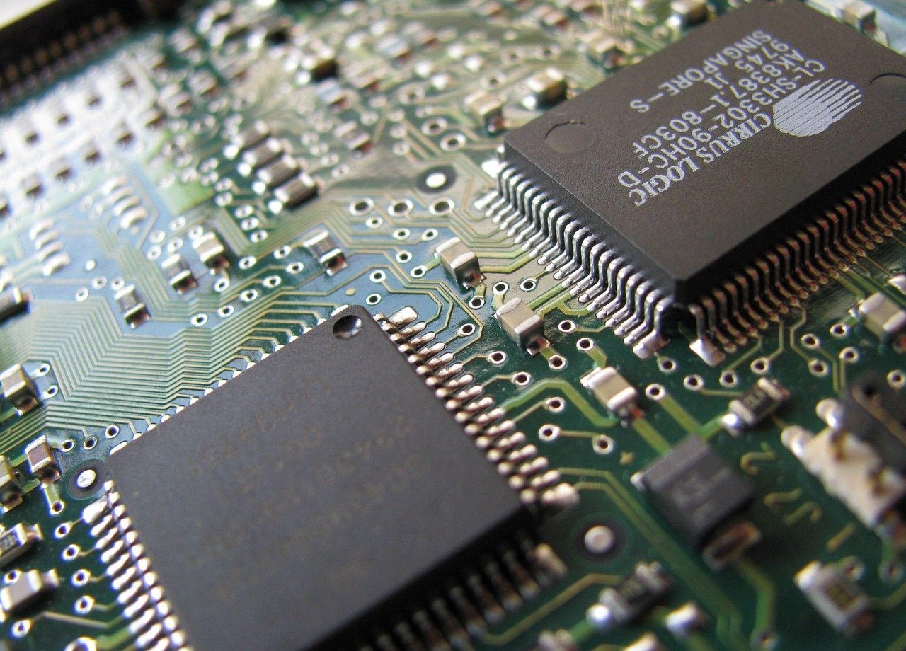
Pad and Footprint Errors
Engineers see problems when pad sizes do not fit leads. If the pad is too small, the solder cannot hold the part. If the pad is too big, solder can connect two pads. These mistakes make more defects. They also make fixing things harder.
Component Placement Problems
Wrong placement of parts causes them to not line up. If parts are too close, they can touch each other. This can make short circuits. Machines may have trouble putting parts in the right spot. Bad design can also cause tombstoning. This is when one end of a chip lifts up.
Stencil and Solder Paste Flaws
Stencil and solder paste problems come from bad design. These problems can cause tombstoning and solder bridges. The table below shows how these problems happen and how to stop them:
Defect Type | How Stencil/Paste Flaws Cause Defects | Solutions |
|---|---|---|
Solder Bridging | If the stencil is not lined up or has too much paste, bridging can happen. | Use the right stencil size and thickness. |
Tombstoning | Not enough paste or uneven heat can make one end lift up. | Use enough paste and heat everything evenly. |
Mechanical and Stress Risks
Designers need to think about stress on the board. Bad design can bend the board or crack solder joints. Heavy parts far from support can make the board bend. This can break the board when people use it. Good design helps the board last longer.
Production and Quality Impact
Defect Rates
Bad design often causes more defects in SMT assembly. If engineers use pads that are the wrong size, problems happen. Parts placed too close together also cause trouble. Machines cannot work right when this happens. Solder bridges and tombstoning show up more often. Parts may not line up as they should. Each defect means someone must check or fix the board. Sometimes, they even have to throw the board away. This extra work makes everything slower. It also means fewer good boards get made.
When there are lots of defects, teams spend more time fixing things. They also have to check quality more often. This means fewer good boards reach the end.
Production Delays
Production slows down when bad design causes problems. Machines stop if they cannot place parts right. Workers have to stop and fix mistakes. Sometimes, they need to change the stencil. They might also need to reprogram the pick-and-place machine. These stops add up and make delivery late.
Delays can happen because of:
Machines stopping a lot
More manual checks
Repairs and rework
Waiting for new parts or stencils
Customers might not get their products on time. This can make people trust the company less. The company might lose business.
Reliability Risks
Boards with bad design can break more easily. Weak solder joints or stressed parts can fail fast. Cracks can form in the solder. Parts might lift off the board. These problems can make the whole product stop working.
Reliability Issue | Cause from Improper Design | Possible Result |
|---|---|---|
Solder Joint Cracks | Pads too small or uneven heating | Intermittent failures |
Component Lift-Off | Poor placement or stress | Complete board failure |
Board Warpage | Lack of support for heavy parts | Broken traces or pads |
People want products that last a long time. If boards break early, people stop trusting the brand.
Cost Impact
Bad design makes costs go up at every step. More defects mean more boards get thrown away. More repairs are needed. Delays make workers spend more time. The company may need to buy new tools or materials. If products fail, the company pays for returns and repairs.
Costs go up because of:
More work to fix boards
Wasted materials
Buying new tools or stencils
Replacing broken products
Companies that use good design save money. They have fewer defects, faster production, and better products.
Preventing Improper Design Effects
Design for Manufacturability
Engineers can stop many problems by using design for manufacturability, or DFM. DFM helps teams make layouts that machines can build well. When designers pick the right pad sizes and leave enough space, machines make fewer mistakes. Good DFM also lowers the chance of tombstoning and solder bridges. Teams that use DFM have fewer defects and finish faster.
Tip: Checking DFM early finds problems before they reach the factory.
Team Collaboration
Good teamwork between design, engineering, and manufacturing helps a lot. When teams talk and share ideas, they find mistakes sooner. Regular meetings help everyone know what each group needs. Designers can learn about machine limits. Production teams can talk about common problems. This teamwork lowers the chance of bad design and saves money later.
Ways to work together better:
Have design reviews with all teams
Share lessons from old projects
Use clear ways to talk to each other
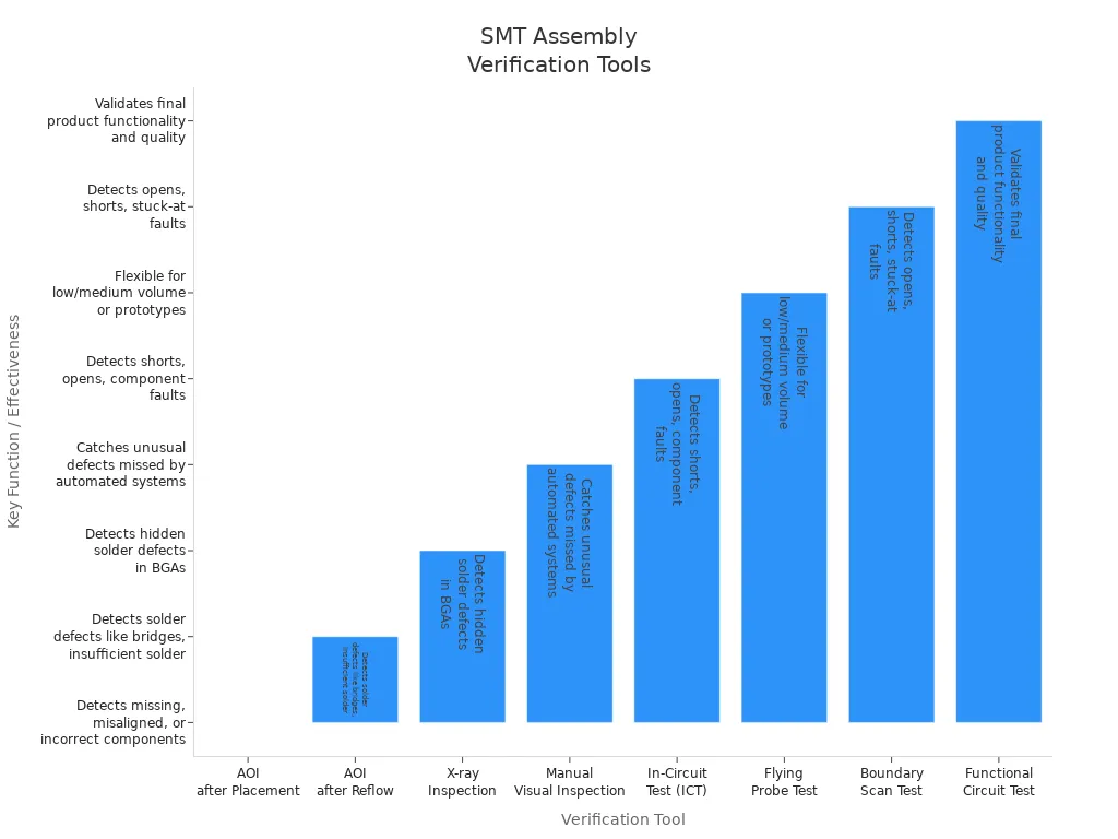
Verification Tools
Verification tools help find mistakes before boards go to customers. Automated Optical Inspection, or AOI, checks for missing or wrong parts. X-ray inspection finds hidden solder problems. Manual checks catch rare mistakes. In-circuit and functional tests make sure boards work right. The table below shows what each tool does:
Verification Tool | Description | Key Functions and Effectiveness |
|---|---|---|
Automated Optical Inspection (AOI) after Placement | Uses high-resolution cameras and image processing to verify component presence, position, and polarity before soldering. | Detects missing, misaligned, or incorrect components early, reducing rework costs and improving assembly quality. |
AOI after Reflow | Inspects solder joint shape, size, and surface characteristics after soldering. | Detects solder defects like bridges, insufficient solder, and tombstoning, ensuring proper solder joint formation. |
X-ray Inspection | Inspects hidden solder joints, especially in BGAs and complex components, before and after reflow. | Detects solder balls, voids, bridges invisible to optical methods; critical for high-reliability applications. |
Manual Visual Inspection | Performed by trained operators using microscopes or magnifying glasses. | Catches unusual defects missed by automated systems; useful for final checks and small production runs. |
In-Circuit Test (ICT) | Uses bed-of-nails fixture to test individual components electrically. | Detects shorts, opens, component faults; provides comprehensive electrical testing and quick fault diagnosis. |
Flying Probe Test | Uses moving probes for electrical testing without custom fixtures. | Flexible for low/medium volume or prototypes; reduces setup time and costs compared to ICT. |
Boundary Scan Test (JTAG) | Tests interconnections between JTAG-compliant devices. | Detects opens, shorts, stuck-at faults; useful for complex, high-density boards; complements other test methods. |
Functional Circuit Test | Verifies PCB performs intended electrical functions under operating conditions. | Detects issues not caught by other tests; validates final product functionality and quality. |
When companies use these tools together, they spend less fixing mistakes and make better boards. New tools like AI and 3D inspection help find even more defects. Teams that use these tools as part of their quality checks avoid many problems from bad design.
SMT assembly teams get more defects and delays when design is poor. Boards can also break more easily. Using DFM and talking with the team helps stop mistakes. These good habits save money and time. Teams that care about design make better products. This also keeps the company’s good name.
Focusing on good design helps save both time and money.
FAQ
What is the most common design mistake in SMT assembly?
Engineers often find pad sizes that are wrong. This mistake makes solder joints weak. It also causes more defects.
How can teams reduce defects from bad design?
Teams follow DFM rules and check designs often. These actions help find mistakes early. They also make boards better.
Why does improper design increase production costs?
Bad design means more fixing, wasted boards, and slow work. Companies pay more for repairs and throw away more parts.
Tip: Checking designs early helps save time and money in SMT assembly.