5 Advanced Testing Methods Used in Professional Through Hole PCB Assembly Services
Ensuring that circuit boards function effectively requires robust testing procedures. Advanced testing methods play a crucial role in identifying issues early and enhancing quality. For instance, heat cycle tests demonstrate that boards can withstand challenging conditions. These methods exceed industry standards. High-quality circuit boards perform better and lead to increased customer satisfaction.
Key Takeaways
Advanced testing finds problems early, improving PCB quality and user happiness.
In-Circuit Testing (ICT) spots 90% of problems fast, saving time and money.
Functional testing copies real-life use, making sure PCBs work well and last longer.
In-Circuit Testing (ICT) in PCB Assembly
Overview of In-Circuit Testing
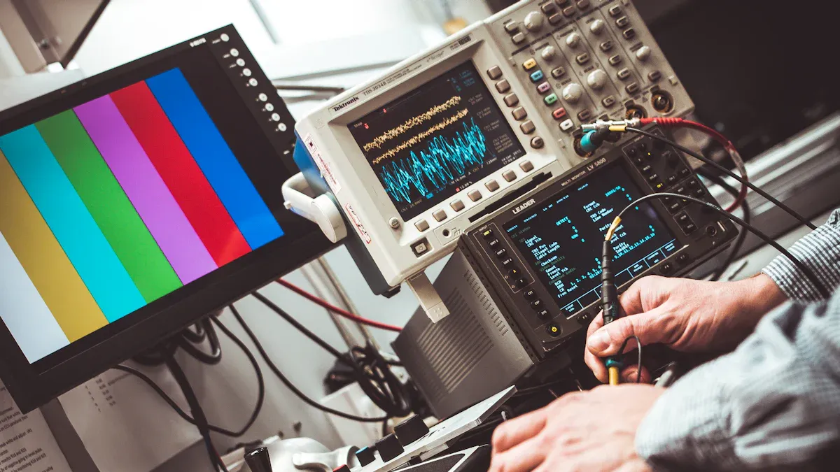
In-circuit testing (ICT) is a trusted way to check circuit boards. It tests each part on the board to ensure it works. ICT uses machines like a bed-of-nails tester or a flying probe tester. These machines touch specific points on the board to run tests. ICT checks for problems like broken connections, wrong tolerances, or short circuits. It ensures every part meets its design needs. By catching issues early, ICT helps avoid bad boards later in production.
Benefits of ICT for Through-Hole PCB Assembly
ICT has many benefits for through-hole PCB assembly. It finds most problems, catching up to 90% of flaws. ICT is also fast, testing many boards at once to save time. It spots about 30% of common issues, like bad soldering or damaged parts. Using ICT lowers repair costs and makes boards more reliable.
Benefit Type | Quantitative Measure |
|---|---|
Defect Detection Rate | Finds about 30% of PCB flaws |
High-Fault Coverage | Detects up to 90% of issues |
Speed | Tests many boards at once |
Applications of ICT in Professional PCB Assembly
ICT is often used in professional PCB testing to check through-hole parts. It tests items like resistors, capacitors, and diodes to ensure they work well. ICT is great for large production runs where speed matters. It also supports advanced tests like boundary scans and analog checks. This makes it useful for complex PCB designs. Adding ICT to your testing process ensures quality and reliable results.
Specification/Metric | Description |
|---|---|
Test Coverage | Includes boundary scans and analog checks. |
Detection Rate | |
Testing Speed | Runs many tests quickly at the same time. |
Component Testing | Checks resistors, capacitors, and diodes. |
Types of Tests | Looks for shorts, opens, and tolerance issues. |
Equipment Used | Uses testers with pins to touch test points. |
Functional Testing for PCB Reliability
What is Functional Testing?
Functional testing checks if a PCB works as planned. It looks at how the board performs based on its design. This testing focuses on what the user experiences, not the internal parts. It’s often called black box testing. Steps include checking power supply, testing ports, and reviewing special features. These steps make sure the board works well in real-world situations.
Component/Step | Description |
|---|---|
Checks voltage levels and power flow. | |
Port (Interface) Test | Finds broken or bad connections. |
Special Functions Testing | Tests unique features made for the board’s design. |
System Control Center | Runs tests and saves results for review. |
Parameter Measurement | Measures signals to confirm they are correct. |
Data Processing and Output | Saves and shares test results for quality checks. |
Why Functional Testing Matters
Functional testing helps keep PCBs reliable. It mimics real-world use to find problems. For example, it tests software, checks system features, and ensures the design works. It also tracks performance over time. Results are recorded to help fix issues and improve designs. This testing repeats the same steps for consistent results. It’s a key part of making sure PCBs work well.
Description | |
|---|---|
Repeatability | Gives the same results every time. |
Versatility | Works for many types of PCB designs. |
Scalability | Fits small or large production needs. |
Continuous Monitoring | Tracks performance while the board is working. |
Reliability | Confirms the board will work over time. |
Traceability | Keeps records of tests for future use. |
Diagnostics | Finds problems with how the board works. |
Data Collection | Gathers info to improve designs later. |
Where Functional Testing is Used
Functional testing is used in many industries to check PCB quality. At LTPCBA, it ensures boards meet top standards. In cars, it tests engine control units with fake inputs like RPM or temperature. In medical devices, it checks patient monitors using pretend bio-signals. Telecom boards are tested for network errors. These examples show how flexible functional testing is. LTPCBA uses it to make sure every project is accurate and reliable.
Industry | Application Description |
|---|---|
Control boards | Tests motor drives and controllers by simulating sensor inputs. |
Telecom boards | Checks network cards for errors and signal quality. |
Power supplies | Measures how converter boards handle changing loads. |
Medical electronics | Tests patient monitors with fake bio-signals. |
Automotive electronics | Checks engine controllers with pretend car inputs like RPM or temperature. |
Avionics boards | Tests navigation systems with GPS-like data. |
IoT Boards | Validates sensing and communication features of smart devices. |
Tip: Functional testing is important for making sure PCBs work correctly. It reduces mistakes and improves reliability.
Automated Optical Inspection (AOI) in PCB Assembly Testing Methods
Introduction to Automated Optical Inspection
Automated Optical Inspection (AOI) is a way to check PCBs without touching them. It uses cameras, special lights, and software to take clear pictures of the board. These pictures are compared to a perfect board to find problems. Issues like bad soldering, missing parts, or broken connections are spotted. AOI gives accurate and steady results, avoiding mistakes people might make.
Advantages of AOI in Detecting Visual Defects
AOI has many benefits for finding PCB problems. It catches issues like solder bridges, open circuits, and misplaced parts. By using machines, it avoids human mistakes and works more precisely. For example, AOI reduces wrong defect alerts by 18% while still finding all real problems. This saves time and improves production. Fixing problems early with AOI costs less than fixing finished boards. It also lowers the need for manual checks, saving money.
Evidence Type | Description |
|---|---|
Fewer false alerts | AOI cuts wrong defect alerts by 18%, keeping 100% accuracy. |
Reliable inspections | AOI checks parts the same way every time, unlike humans. |
Cost savings | Finding problems early with AOI saves money on repairs and labor. |
Scenarios Where AOI is Most Effective
AOI works best in certain steps of PCB testing. After soldering, it finds weak solder spots that might fail. For boards with many parts, it checks if everything is in the right place. It also spots solder bridges that connect parts by mistake. Some AOI systems can check both sides of a board at once, which is great for crowded designs. This saves repair costs and ensures high-quality boards.
Scenario | Type of Defect | Description |
|---|---|---|
After soldering | Weak solder joints | Finds spots where solder isn’t strong enough. |
For complex boards | Missing parts | Makes sure all parts are in place. |
During assembly | Solder bridges | Spots unwanted solder connections. |
Early problem detection | Open circuits | Finds breaks that stop electricity from flowing. |
Tip: Adding AOI to your testing process improves quality, saves money, and finds defects faster.
X-Ray Inspection for Advanced Testing Methods
What is X-Ray Inspection?
X-ray inspection is a way to check inside a PCB without breaking it. It uses clear images to find hidden problems like gaps, misplaced parts, or solder mistakes. This method works well for checking tricky boards, like ones with Ball Grid Arrays (BGAs) or many layers. By looking at the inside layers, you can make sure the PCB works properly and lasts a long time.
Benefits of X-Ray Inspection in Through-Hole PCB Assembly
X-ray inspection has many benefits for through-hole PCB assembly.
Non-Destructive Testing: It checks delicate parts without harming the board, which is great for expensive projects.
Detailed Imaging: Sharp images help spot important issues like gaps, solder errors, or misaligned parts.
Enhanced Accuracy: Smart systems using AI can find 99.9% of defects, better than human checks.
This method is very useful for keeping complex boards high-quality, especially as designs get harder to inspect.
Applications of X-Ray Inspection in Complex PCB Designs
X-ray inspection is key for studying complicated PCB designs. It’s often used to find problems in BGAs and layered boards where other methods don’t work well. For example, Foxconn’s AI tools can detect solder problems smaller than 10 microns with 99.7% accuracy.
Inspection Type | Advantages | Limitations |
|---|---|---|
Finds hidden solder issues; Good for BGA parts; Doesn’t harm the board | Limited depth info; Costs more than visual checks; Needs skilled operators | |
3D X-ray | Gives detailed 3D views of solder joints; Spots gaps, bridges, and inside problems; Very accurate for tough designs | Costs more than 2D X-ray; Takes longer; Needs advanced software and trained users |
Adding X-ray inspection to your testing process helps find more defects and ensures top-quality PCBs.
Burn-In Testing for Long-Term Reliability
What is Burn-In Testing?
Burn-in testing checks if a PCB can handle tough conditions. It puts the board under stress, like high heat, voltage, and current. This test mimics harsh environments to find hidden problems.
Main factors in burn-in testing include:
Temperature: Heat speeds up aging and shows heat-related problems.
Voltage and Current: Higher levels test parts for weak spots.
Cycles: Turning power on and off copies real-world use.
Environmental Factors: Tests like humidity or interference check durability.
This process ensures only strong PCBs are sold, lowering early failures.
How Burn-In Testing Improves Reliability
Burn-in testing makes PCBs more reliable by finding hidden flaws. It pushes the board to its limits to reveal weak parts or bad soldering. For example, heating and cooling cycles show cracks in solder or materials. Fixing these problems early ensures the board works well in real life.
Tips for Effective Burn-In Testing
To get the best results, follow these tips:
Test in hot environments to catch early part failures.
Use heat and cold cycles to find weak spots.
Check the board’s performance across all temperature ranges.
Make sure solder joints and materials stay strong under stress.
By following these steps, you’ll create reliable PCBs that meet customer needs.
Modern testing methods help find problems early and improve quality. Pick a testing method that fits your PCB needs, like size or quantity. Working with LTPCBA ensures expert PCB services and dependable outcomes for your work.
FAQ
Why is through-hole PCB assembly dependable?
Through-hole PCB assembly creates strong connections. It handles stress and shaking better than other methods. This makes it great for important uses like cars and airplanes.
How do testing methods lower defects?
Testing finds problems early in production. Fixing issues before the final step saves time and money. It also helps make sure PCBs work well.
Why choose LTPCBA for PCB assembly?
LTPCBA uses smart tools, strict checks, and quick service. Their skills make them reliable for small projects and big production runs.
See Also
Essential Quality Control Steps for Through Hole PCB Assembly
In-Depth Overview of Through Hole PCB Assembly Techniques
Evaluating Reliability: Through Hole PCB Assembly Versus SMT
Selecting the Ideal All-in-One PCB Assembly Provider
Guidelines for Selecting Through Hole PCB Assembly for Industry